2015年 第1卷 第3期
《工程(英文)》 >> 2015年 第1卷 第3期 doi: 10.15302/J-ENG-2015052
基于高κ/GaAs界面态起源的材料设计
1 Department of Materials Science and Engineering, The University of Texas at Dallas, Richardson, TX 75080, USA
2 College of Electronic Information and Optical Engineering, Nankai University, Tianjin 300071, China
下一篇 上一篇
摘要
为了满足微电子器件不断扩展到更小尺寸的需求,SiO2栅极介电层被高介电常量材料Hf(Zr)O2所替代,以尽可能减少流过介电薄膜的漏电流。然而,与高介电常量 (高κ) 电介质连接时,传统Si通道中的电子迁移率由于库仑散射、表面粗糙度散射、远程声子散射和介电电荷捕获而有所下降。III-V和Ge是两个有希望的候选材料,其迁移率均优于Si。尽管如此,与Si基界面相比,Hf(Zr)O2/III-V(Ge) 的界面结合更为复杂。成功制造高质量器件关键在于优化器件界面设计时对Hf(Zr)O2/III-V(Ge) 界面结合结构的理解与设计。因此,从原子尺度准确了解界面结合与界面态形成的机制变得尤为重要。在本文中,笔者利用第一性原理计算方法,对HfO2与GaAs之间的界面性质进行了研究。结果表明,隙间态主要由As—As二聚物键合、Ga部分氧化( 在3+和1+之间) 和Ga—悬挂键贡献。这些研究成果能为最优化界面钝化提供重要的指导意见。
图片
图1
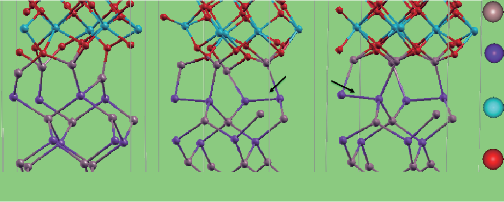
图2
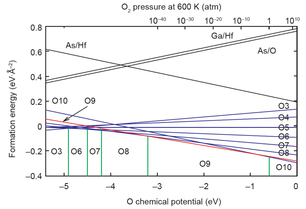
图3

图4

图5
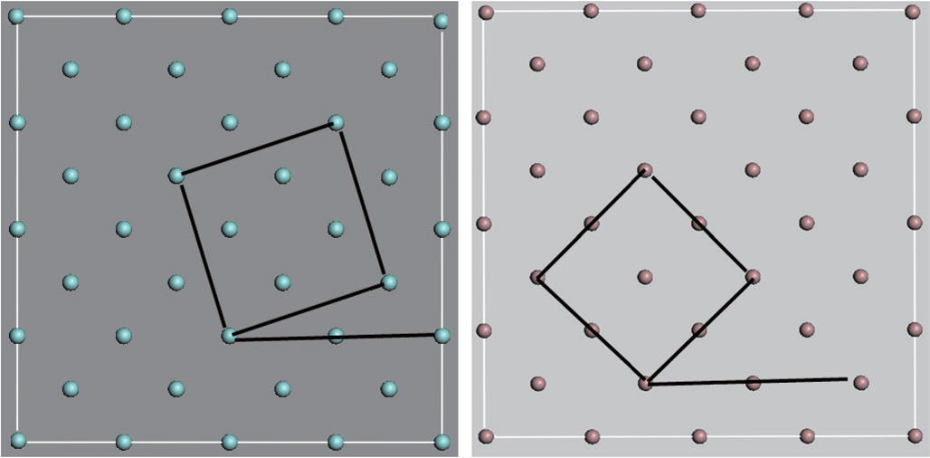
图6
参考文献
[ 1 ] J. Robertson, R. M. Wallace. High-k materials and metal gates for CMOS applications. Mat. Sci. Eng. R., 2015, 88: 1–41
[ 2 ] K. Cho. First-principles modeling of high-k gate dielectric materials. Comp. Mater. Sci., 2002, 23(1−4): 43–47 链接1
[ 3 ] M. Haverty, A. Kawamoto, K. Cho, R. Dutton. First-principles study of transition-metal aluminates as high-k gate dielectrics. Appl. Phys. Lett., 2002, 80(15): 2669–2671 链接1
[ 4 ] S. Park, L. Colombo, Y. Nishi, K. Cho. Ab initio study of metal gate electrode work function. Appl. Phys. Lett., 2005, 86(7): 073118 链接1
[ 5 ] J. H. Ha, P. C. McIntyre, K. Cho. First principles study of the HfO2/SiO2 interface: Application to high-k gate structures. J. Appl. Phys., 2007, 101(3): 033706
[ 6 ] The White House. About the Materials Genome Initiative. https://www.whitehouse.gov/mgi
[ 7 ] B. Lee, K. Cho. Extended embedded-atom method for platinum nanoparticles. Surf. Sci., 2006, 600(10): 1982–1990 链接1
[ 8 ] X. Hao, Experimental and theoretical study of CO oxidation on PdAu catalysts with NO pulse effects. Top. Catal., 2009, 52(13−20): 1946–1950 链接1
[ 9 ] B. Shan, First-principles-based embedded atom method for PdAu nanoparticles. Phys. Rev. B, 2009, 80(3): 035404
[10] M. J. Hale, S. I. Yi, J. Z. Sexton, A. C. Kummel, M. Passlack. Scanning tunneling microscopy and spectroscopy of gallium oxide deposition and oxidation on GaAs(001)-c(2×8)/(2×4). J. Chem. Phys., 2003, 119(13): 6719–6728
[11] D. L. Winn, M. J. Hale, T. J. Grassman, A. C. Kummel, R. Droopad, M. Passlack. Direct and indirect causes of Fermi level pinning at the SiO/GaAs interface. J. Chem. Phys., 2007, 126(8): 084703
[12] M. Passlack, R. Droopad, P. Fejes, L. Wang. Electrical properties of Ga2O3/GaAs interfaces and GdGaO dielectrics in GaAs-based MOSFETs. IEEE Electr. Device L., 2009, 30(1): 2–4 链接1
[13] C. L. Hinkle, Comparison of n-type and p-type GaAs oxide growth and its effects on frequency dispersion characteristics. Appl. Phys. Lett., 2008, 93(11): 113506 链接1
[14] C. L. Hinkle, M. Milojevic, E. M. Vogel, R. M. Wallace. The significance of core-level electron binding energies on the proper analysis of InGaAs interfacial bonding. Appl. Phys. Lett., 2009, 95(15): 151905 链接1
[15] R. V. Galatage, Accumulation capacitance frequency dispersion of III-V metal-insulator-semiconductor devices due to disorder induced gap states. J. Appl. Phys., 2014, 116(1): 014504 链接1
[16] M. Passlack, M. Hong, J. P. Mannaerts, S. N. G. Chu, R. L. Opila, N. Moriya. In-situ Ga2O3 process for GaAs inversion/accumulation device and surface passivation applications. In: 1995 International Electron Devices Meeting. Piscataway, NJ: IEEE, 1995: 383–386
[17] E. P. O’Reilly, J. Robertson. Electronic structure of amorphous III-V and II-VI compound semiconductors and their defects. Phys. Rev. B Condens. Matter, 1986, 34(12): 8684–8695 链接1
[18] P. W. Peacock, J. Robertson. Bonding, energies, and band offsets of Si-ZrO2 and HfO2 gate oxide interfaces. Phys. Rev. Lett., 2004, 92(5): 057601 链接1
[19] J. Robertson, L. Lin. Fermi level pinning in Si, Ge and GaAs systems—MIGS or defects? In: 2009 International Electron Devices Meeting. Piscataway, NJ: IEEE, 2009: 119
[20] W. Wang, K. Xiong, R. M. Wallace, K. Cho. Impact of interfacial oxygen content on bonding, stability, band offsets, and interface states of GaAs:HfO2 interfaces. J. Phys. Chem. C, 2010, 114(51): 22610–22618 链接1
[21] C. L. Hinkle, E. M. Vogel, P. D. Ye, R. M. Wallace. Interfacial chemistry of oxides on InxGa(1–x) As and implications for MOSFET applications. Curr. Opin. Solid St. M., 2011, 15(5): 188–207 链接1
[22] K. Kukli, M. Ritala, T. Sajavaara, J. Keinonen, M. Leskelä. Atomic layer deposition of hafnium dioxide films from hafnium tetrakis(ethylmethylamide) and water. Chem. Vapor. Depos., 2002, 8(5): 199–204 链接1
[23] S. Keun Kim, C. Seong Hwang, S. H. Ko Park, S. Jin Yun. Comparison between ZnO films grown by atomic layer deposition using H2O or O3 as oxidant. Thin Solid Films, 2005, 478(1−2): 103–108 链接1
[24] G. Henkelman, A. Arnaldsson, H. Jónsson. A fast and robust algorithm for Bader decomposition of charge density. Comp. Mater. Sci., 2006, 36(3): 354–360 链接1
[25] J. Robertson. Model of interface states at III-V oxide interfaces. Appl. Phys. Lett., 2009, 94(15): 152104 链接1
[26] W. Wang, G. Lee, M. Huang, R. M. Wallace, K. Cho. First-principles study of GaAs (001)-β2 (2 × 4) surface oxidation and passivation with H, Cl, S, F, and GaO. J. Appl. Phys., 2010, 107(10): 103720
[27] W. Wang, K. Xiong, C. Gong, R. M. Wallace, K. Cho. Si passivation effects on atomic bonding and electronic properties at HfO2/GaAs interface: A first-principles study. J. Appl. Phys., 2011, 109(6): 063704
[28] J. Robertson. Band offsets of wide-band-gap oxides and implications for future electronic devices. J. Vac. Sci. Technol. B, 2000, 18(3): 1785–1791
[29] G. D. Wilk, R. M. Wallace, J. M. Anthony. High-κ gate dielectrics: Current status and materials properties considerations. J. Appl. Phys., 2001, 89(10): 5243–5275
[30] C. G. van de Walle, R. M. Martin. Theoretical study of band offsets at semiconductor interfaces. Phys. Rev. B Condens. Matter, 1987, 35(15): 8154–8165 链接1
[31] H. M. Al-Allak, S. J. Clark. Valence-band offset of the lattice-matched β-FeSi2(100)/Si(001) heterostructure. Phys. Rev. B, 2001, 63(3): 033311
[32] V. V. Afanas’ev, Energy barriers at interfaces of (100)GaAs with atomic layer deposited Al2O3 and HfO2. Appl. Phys. Lett., 2008, 93(21): 212104 链接1
[33] G. Seguini, M. Perego, S. Spiga, M. Fanciulli, A. Dimoulas. Conduction band offset of HfO2 on GaAs. Appl. Phys. Lett., 2007, 91(19): 192902 链接1
[34] G. K. Dalapati, H. J. Oh, S. J. Lee, A. Sridhara, A. S. W. Wong, D. Chi. Energy-band alignments of HfO2 on p-GaAs substrates. Appl. Phys. Lett., 2008, 92(4): 042120 链接1
[35] J. Robertson, B. Falabretti. Band offsets of high K gate oxides on III-V semiconductors. J. Appl. Phys., 2006, 100(1): 014111
[36] A. G. Cullis, L. T. Canham. Visible light emission due to quantum size effects in highly porous crystalline silicon. Nature, 1991, 353(6342): 335–338 链接1
[37] V. Lehmann, U. Gösele. Porous silicon formation: A quantum wire effect. Appl. Phys. Lett., 1991, 58(8): 856–858 链接1
[38] J. Zhu, Z. G. Liu. Structure and dielectric properties of ultra-thin ZrO2 films for high-k gate dielectric application prepared by pulsed laser deposition. Appl. Phys. A-Mater., 2004, 78(5): 741–744 链接1
[39] C. L. Hinkle, GaAs interfacial self-cleaning by atomic layer deposition. Appl. Phys. Lett., 2008, 92(7): 071901 链接1
[40] C. L. Hinkle, Detection of Ga suboxides and their impact on III-V passivation and Fermi-level pinning. Appl. Phys. Lett., 2009, 94(16): 162101 链接1
[41] W. H. Press, B. P. Flannery, S. A. Teukolsky, W. T. Vetterling. Numerical Recipes: The Art of Scientific Computing. New York: Cambridge University Press, 1986
[42] J. P. Perdew, M. Ernzerhof, K. Burke. Rationale for mixing exact exchange with density functional approximations. J. Chem. Phys., 1996, 105(22): 9982–9985
[43] P. Hohenberg, W. Kohn. Inhomogeneous electron gas. Phys. Rev., 1964, 136(3B): B864–B871 链接1
[44] W. Kohn, L. J. Sham. Self-consistent equations including exchange and correlation effects. Phys. Rev., 1965, 140(4A): A1133–A1138 链接1
[45] J. P. Perdew, K. Burke, M. Ernzerhof. Generalized gradient approximation made simple. Phys. Rev. Lett., 1996, 77(18): 3865–3868 链接1
[46] L. C. West, S. J. Eglash. First observation of an extremely large-dipole infrared transition within the conduction band of a GaAs quantum well. Appl. Phys. Lett., 1985, 46(12): 1156–1158 链接1


 京公网安备 11010502051620号


