

《1. Introduction》
1. Introduction
Large-scale information monitoring is one of the foundations for the realization of smart grids and the energy internet [1–3]. Through the large-scale collection of voltage and current data, a control strategy for power systems can be optimized, and status monitoring and fault diagnosis of power systems and equipment can be realized [4]. High voltage is traditionally measured by a voltage transformer, which is bulky and has poor performance. Moreover, the need for insulation increases the cost of measurement and the difficulty of operation and maintenance. Given the need for an increasing number of sensing nodes, such largevolume and high-cost voltage-measuring equipment can no longer meet the demand. According to the Gauss–Legendre algorithm, voltage can be reversed by measuring the electric field at several points [5,6]. Therefore, with the use of an electric field sensor (E-sensor), non-contact voltage measurement can be realized, which can reduce the cost of measurement and increase the quantity of sensing nodes [7,8]. In addition to voltage measurement, Esensors can be used for the fault monitoring of electrical equipment [9–11]. It is difficult to implement status monitoring and fault diagnosis of electrical equipment online. When insulation failure or partial discharge occurs in electrical equipment, the internal electric field of the equipment will change. By arranging micro-E-sensors and extracting fingerprint characteristics of the electric field signal, such faults can be monitored and diagnosed online.
E-sensors have important applications in fields other than power systems as well, as shown in Fig. 1 [12]. Wearable Esensors can be used for near-electricity warnings for electric workers [13]. E-sensors can also be used to monitor the electric field of the atmospheric, in order to realize lightning warning, weather forecasting, and the selection of space launch windows [14–17]. Furthermore, measurement of the electrostatic field can be used in industrial production as a means of safety monitoring, especially in the petrochemical industry. In addition, E-sensors can be used for cabin monitoring in advanced electric vehicles and aircraft [18]. Application in such areas requires E-sensors to have high resolution, a wide measurable range, and low power consumption, in addition to a small size and low cost.
《Fig. 1》

Fig. 1. Applications of micro-E-sensors. E: electric field.
At present, electric field measurement presents numerous difficulties. For one thing, large and high-permittivity measuring devices will cause electric field distortion. For another, a complex electromagnetic environment often results in high coupling interference. In a power system, the amplitude of electric field measurement can reach the order of megavolts per meter, and the measurement frequency varies from direct current (DC) to kilohertz. At the same time, in order to meet the needs of most application scenarios in a power grid, the resolution of electric field measurement must be within 200 V·m–1 . Field mills are traditionally used in the measurement of electric fields. However, due to the large size and low accuracy, this approach can no longer meet current needs. Microsensors are small advanced sensors with a low cost and high performance that can easily be mass produced using microfabrication technology. The principles behind micro-Esensors include the electro-optical effect, charge induction, and the piezoelectric effect. The measurement of optical E-sensors is based on the change in the refractive index of electro-optic crystals under electric fields [19–23]. Optical E-sensors have a high resolution and wide frequency bandwidth and are currently used in applications such as bus voltage measurement in substations. Although such E-sensors are small, they need to be connected to expensive and bulky light sources and receivers through optical fibers, which cannot be arranged flexibly in equipment or on a large scale.
Electric fields can also be measured using the induced charges of a conductor in an electric field [24–27]. Micro-electromechanical system (MEMS) E-sensors based on charge induction are composed of a vibrating shield electrode, a fixed electrode for inducing charge, and back-end circuits. Such sensors have the advantages of small size and low cost. However, they often introduce high noise interference, and it is difficult to improve their frequency response and resolution, due to the limitations of their sensing area. Micro-E-sensors based on the piezoelectric effect measure electric fields by sensing the deformation of piezoelectric materials under an electric field [28–31]. Such E-sensors are small and can be easily integrated. Nevertheless, the fabrication technology for piezoelectric materials and issues with the sensor performance—such as resolution and the signal-to-noise ratio—limit the application of such sensors.
In this paper, we present an electrostatically actuated microE-sensor with a piezoresistive sensing structure. The sensor is fabricated into a four-cantilever structure with grounded metal films arranged at the ends of the cantilevers. Driven by electrostatic force, the cantilevers bend up in an electric field. The strain generated by the bending of the cantilever causes a change in the resistance of the piezoresistive materials at the roots of the cantilevers. The electric field is measured according to the output signal of a Wheatstone bridge circuit with piezoresistive materials arranged on its arms. Compared with optical E-sensors, the presented Esensor has a small size of 8 mm × 8 mm and can be mass produced at a low cost using silicon-based microfabrication technology. Compared with MEMS E-sensors, the presented E-sensor does not require additional shielded electrode drive sources. In addition, since the response frequency of the E-sensor is twice the frequency of the electric field, the coupling interference of the E-sensor can be effectively reduced. Moreover, because the harmonics in the power grid are mostly odd harmonics, the output signal at a double frequency makes the sensor more suitable for power systems. The experimental results show that the cut-off frequency of the Esensor is as high as 496 Hz, and the measurable electric field ranges from 1.1 to 1100.0 kV·m–1 with an alternating current (AC) resolution of 112 V·m–1 ·Hz–1/2. The performance of the presented Esensor meets most of the application requirements for smart grids and the energy internet.
《2. Working principle and structural design》
2. Working principle and structural design
When a metal film is placed in an electric field, the free charge carriers will redistribute, resulting in opposite charges at the surface of the metal film, as shown in Fig. 2(a). This polarization compensates for the electric field inside the metal. In an external electric field, these generated charges are subject to an outward electrostatic field force, while the resultant force on the metal film remains at zero. If the lower surface of the metal film is grounded, the charges generated on the lower surface are transferred away, and the metal film is subject to an upward electrostatic force. When a metal film is prepared on the free end of a silicon cantilever, the cantilever will bend up under the drive of the metal film, as shown in Fig. 2(b). The electrostatic force (Fes) on the metal film can be calculated as follows:

where A is the area of the metal film, E is the electric field along the normal direction of the film, and ε is the dielectric constant of air.
《Fig. 2》

Fig. 2. Response of a silicon cantilever with metal film in an electric field. (a) Induced charges of the metal film; (b) force of the grounded metal film and displacement of the silicon cantilever. Fes: electrostatic force.
The structure of the presented E-sensor is shown in Fig. 3. The sensor is designed as a four-cantilever structure, where the four cantilevers are symmetrically distributed. One end of each cantilever is fixed in the center of the silicon substrate column, while the other end of the cantilever can vibrate freely. A grounded metal film is prepared on the free end of each cantilever. Under the action of an electric field, the four cantilevers bend up with the same amplitudes, as shown in Fig. 3(a), generating stress inside the silicon cantilevers. At the fixed end of the cantilevers, four zigzag piezoresistive areas are prepared using ion doping. The piezoresistive areas are connected by metal electrodes to form a Wheatstone bridge circuit, as shown in Fig. 3(b).
《Fig. 3》

Fig. 3. Structure of the E-sensor. (a) Diagram of the E-sensor structure; (b) overhead view of the E-sensor structure and circuit. GND: ground; R1–R4: piezoresistive areas; Us: constant voltage source; Uo: output voltage.
When the strain of the four silicon cantilevers changes, the energy band of the doped silicon also changes, moving the energy of the energy valley. The stress of the doped silicon satisfies the following:

where  is the stress along the length of the cantilever,
  is the stress perpendicular to the length of the cantilever, and
  is the Poisson ratio of the doped silicon.
Under the silicon strain, the resistance of the four piezoresistive areas changes. Among the four piezoresistive areas, R1 and R3 are designed as a zigzag shape, which couples the strain along the length of the cantilever. R2 and R4 are designed as a straight strip shape, which couples the strain along the width of the cantilever. Thus, the resistance changes of the adjacent piezoresistive areas are reversed. The initial resistance values of the piezoresistive areas are designed to be the same to reduce zero drift. If we set the initial resistance of the four piezoresistive areas as R0 and mark the resistivity changes in R1 and R3 as  and the resistivity changes in R2 and R4 as
  , then:

where  and
and  are the piezoresistive coefficients in the longitudinal and transverse directions, respectively. In the designed E-sensor, the values of and are +71.3 and –66.7, respectively. P(N, T) is the coefficient that depends on the semiconductor doping density N and the temperature T.
When applying a constant voltage source Us at the input ports Us(+) and Us(–) of the Wheatstone bridge, according to Kirchhoff’s laws, the output of the Wheatstone bridge Uo can be calculated as follows:

According to Eq. (4), under fixed doping conditions, the piezoresistive areas where the strain is the largest should be selected to increase the response of the E-sensor.
To verify the working principle of the presented E-sensor, we use the finite-element method (FEM) via Comsol Multiphysics to simulate the E-sensor response under different parameters and electric fields. To simplify the model, the surrounding fixed area of the E-sensor is omitted, while the fixed silicon column and four cantilevers are retained. The simulation uses the physics of electrostatics and solid mechanics and the multiphysics of electromechanical force. We set the cantilever to free boundary conditions. The boundary conditions of other areas are fixed. Fig. 4 shows the response of the E-sensor when an electric field of 1 MV·m–1 is applied along the z-axis.
Figs. 4(a) and (b) show the distribution of the cantilever displacement. Under the electrostatic force, the metal film at the end of the cantilever drives the cantilever to bend upward. The four cantilevers have the same displacement. It is worth noting that the force on the cantilever is always upward, regardless of whether the direction of the electric field is along the positive or negative z-axis. Figs. 4(c) and (d) shows the distribution of the XX strain component on the cantilever. The YY strain component is symmetrical with the XX component. As shown in the figure, the largest strain component on the cantilever is located at the root of the cantilever. In order to maximize the sensor response, the ion-doped area is chosen to be close to the fixed area on the cantilever.
《Fig. 4》

Fig. 4. Simulated response of the E-sensor. (a) Distribution of the displacement; (b) displacement curve of the cantilever; (c) distribution of the strain tensor XX (eXX); (d) cantilever curve for the strain tensor XX.
According to simulations, the maximum strain of the E-sensor increases linearly with the electric field. When the electric field is applied in the reverse direction along the z-axis, the sensor response is the same as the electric field is applied along the z-axis. In addition, the response of the E-sensor is related to the length and thickness of the cantilever. Simulations can provide a theoretical reference for designing the optimal parameters and layout of the E-sensor. Increasing the maximum strain of the cantilever under the same electric field can increase the output of the Wheatstone bridge, thereby increasing the resolution of the E-sensor. The relationship between the maximum strain tensor XX (eXX) on the cantilever and the length and thickness of the cantilever is shown in Fig. 5.
《Fig. 5》

Fig. 5. Relationship between the maximum strain tensor XX on the cantilever and the length and thickness of the cantilever. (a) Maximum strain tensor XX under different cantilever lengths  ; (b) maximum strain tensor XX under different cantilever thicknesses Tc.
According to the principle of leverage, under the same electrostatic force, increasing the length of the cantilever increases the torque. Therefore, under the same electric field, the longer the cantilever is, the greater the maximum strain on the cantilever will be, as shown in Fig. 5(a). Within a reasonable range, increasing the cantilever length improves the response of the E-sensor. However, an excessive cantilever length both reduces the mechanical strength of the cantilever and makes it more difficult to prepare the device. Moreover, as the length of the cantilever increases, the resonant frequency of the cantilever drops, causing the cutoff frequency of the E-sensor to decrease. Considering various factors such as device fabrication, lifetime, and device performance, the length of the fabricated E-sensor cantilever was selected to be within the range of 1250–2250 μm.
Similarly, reducing the thickness of the cantilever increases the maximum strain on the cantilever, thereby increasing the E-sensor response, as shown in Fig. 5(b). However, a cantilever that is too thin will affect the fabrication difficulty and mechanical strength of the E-sensor. Thus, the cantilever thickness of our E-sensor was chosen to be 5 and 10 μm.
Changing the metal film area affects the sensor response. According to Eq. (1), increasing the metal film area A increases the electrostatic force, thus increasing the sensor response. Therefore, the area of the metal film should be as large as possible. However, when the length of the metal film increases past a certain value, the increase in the sensor response becomes insignificant. Moreover, when the metal is close to the root of the cantilever, it may affect the fabrication of the piezoresistive material. Therefore, the metal film was fabricated at the end of the cantilever, and a length of 800 μm was chosen. Section 4 shows a performance comparison of E-sensors with different parameters.
《3. Device fabrication》
3. Device fabrication
Based on the theoretical analysis and simulation results of the designed E-sensor structure, the presented E-sensor was fabricated using silicon-based microfabrication technology. The fabrication process was based on 10 cm diameter silicon-on-insulator (SOI) wafers with a device layer thickness of 5 and 10 μm and a box thickness of 1 μm. The crystal orientation of the device layer was selected to be and the resistivity of the device silicon was 6–8 Ω·cm. About 90 E-sensors can be produced on one 10 cm diameter wafer.
A schematic illustration of the E-sensor fabrication process is provided in Fig. 6. The wafer is patterned and fabricated through a combination of photolithography technology and other microfabrication technologies. The six photolithography masks used in the fabrication process are shown in Fig. 7(a). After the SOI wafer is cleaned with a mixture of hot concentrated sulfuric acid and hydrogen peroxide, the piezoresistive area is patterned onto the device layer. In order to ion dope the piezoresistive area, the wafer is heated in an oxygen atmosphere to form a 20 nm silicon oxide layer on the surface. The oxide layer acts as a shielding layer for the ion doping. Next, boron ions are doped onto the device layer with a concentration of 5 × 1018 cm–3 , forming a PN junction with a depth of 1.5 μm. The piezoresistive areas are created within the designed shape using photolithography, and ohmic contact areas are provided to ensure good ohmic contact between the piezoresistive areas and the electrodes. The wafer is annealed at 1000 °C for 30 min in a nitrogen atmosphere to activate the doped areas. After the piezoresistive areas are fabricated, a silicon oxide insulating layer with a thickness of 400 nm is grown on the surface of the wafer in an oxygen atmosphere. The insulating layer is then patterned using inductively coupled plasma (ICP) etching technology to release the silicon oxide in the ohmic contact area and the cantilever area. Finally, a metal layer composed of a chromium (Cr) layer and a gold (Au) layer is prepared on the surface of the device layer by means of magnetron sputtering. The metal is patterned into a Wheatstone bridge shape using photolithography and wet etching. In this way, the processing of structure on the device layer surface is completed.
《Fig. 6》

Fig. 6. Schematic illustration of the E-sensor fabrication. PCB: printed circuit board.
Processing in the depth direction of the wafer is then performed. First, the device layer is patterned using ICP etching to form the shape of the cantilevers. Then, the handle layer under the cantilever structure is etched away. Finally, the box layer is etched away to release the four cantilevers. During the cantilever release, the temperature and time of the processing must be accurately controlled to ensure that the cantilevers have the same initial state. The fabricated wafer before dicing is shown in Fig. 7(b). The microstructure of the sensor chip is shown in Fig. 7(c).
《Fig. 7》
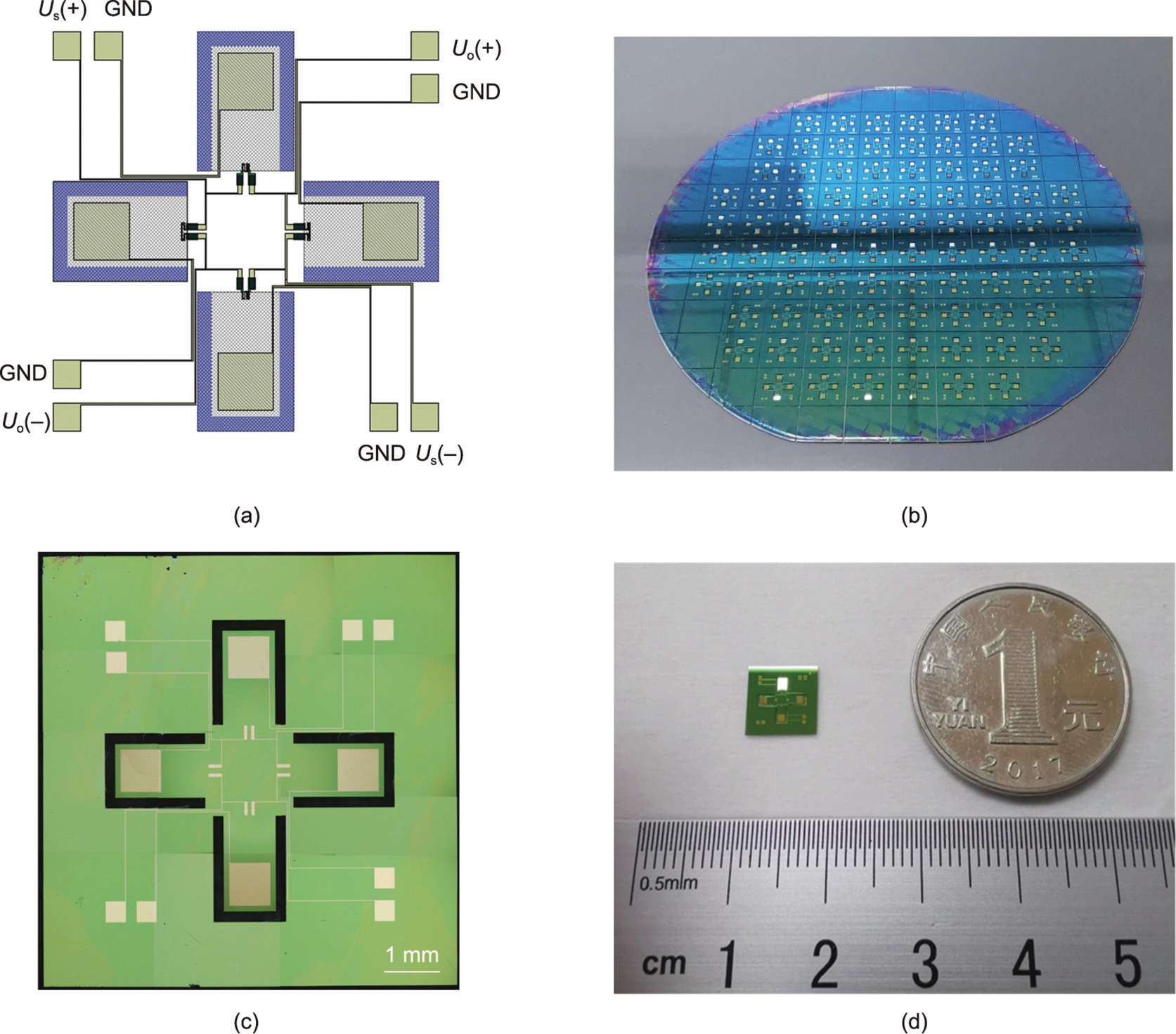
Fig. 7. The fabricated micro-E-sensor. (a) Masks for photolithography; (b) overall view of the 10 cm diameter wafer before dicing; (c) microscopic image of the Esensor structure; (d) diagram showing the E-sensor size.
Finally, the wafer is diced into 8 mm × 8 mm chips using laser cutting, as shown in Fig. 7(d). The metal electrodes on the E-sensor are welded to the printed circuit board (PCB) with gold wire. As discussed in Section 4, the PCB was used in an electric field test station to further test the E-sensor performance.
《4. Device performance》
4. Device performance
An electric field test station was built for the performance testing of the E-sensors, as shown in Fig. 8(a). The test station can generate electric fields with different field strengths, frequencies, and waveforms. In the test station, an electric field is generated by applying a voltage to a pair of circular metal electrodes. The ratio of the electrode diameter to the distance should be high enough to ensure a uniform electric field between the electrodes. A column for fixing the PCB board is arranged beside the two electrodes. The PCB board is designed as a ‘‘T” shape, as shown in Fig. 8(b). The Esensor is placed on one end of the PCB, and the other end of the PCB is fixed by screws. The input voltage signal is generated by a generator (DG1022, Rigol Technology Inc., China) and amplified by a high-voltage amplifier (TREK MODEL 10/10B-HS, Trek Inc., USA) with a fixed gain of 1000. The output signal of the sensor is differentially amplified by the back-end circuit based on AD623, as shown in Fig. 8(c). The back-end circuit is arranged on the PCB. The amplified signal is used for frequency selection through a lock-in amplifier (MFLI, Zurich Instruments, Switzerland), based on a generator signal frequency twice as high as the synchronization signal frequency. In addition, a high-precision voltage source (B2912A, Keysight Technology Inc., USA) is used to provide a 6 V input signal to the Wheatstone bridge on the sensor chip. Based on a LabVIEW program, the output signal of the generator and the output of the lock-in amplifier are controlled and collected through a personal computer (PC).
《Fig. 8》

Fig. 8. Electric field measurement setup. (a) Schematic of the electric field measurement setup; (b) schematic of the PCB; (c) back-end differential amplification circuit. PC: personal computer; sync: synchronization signal;  : frequency of generator signal; RG: external gain setting resistor, Vin: input signal, Vout: output signal, VREF: output reference signal, Vs: positive supply terminal.
Based on the electric test station, we tested the prepared Esensors with different parameters under electric fields with different amplitudes and frequencies. The tests were carried out under stable environmental conditions with the air pressure maintained at 101 kPa, the temperature at (25 ± 1) °C, and the humidity at 50 ± 10%. For electric field measurement, important parameters include the dynamic range, linearity, cut-off frequency, and resolution. The fabricated E-sensors were divided into four groups, marked as S1, S2, S3, and S4. Each group consisted of 10 sensor chips. The cantilever lengths of the E-sensors were 1250, 1750, and 2250 μm, respectively. The cantilever thickness of the Esensors was set to 5 and 10 μm. Table 1 displays the performance of E-sensors with different parameters.
The four groups of E-sensors were tested under different electric field strengths at 50 Hz. The output voltages of the E-sensors are shown in Fig. 9(a). At a fixed frequency, the amplitude response of the E-sensors exhibits high linearity. The output voltage curve is linearly fitted, and the coefficient of determination (r2 ) values of Sensors S1–S4 are 0.998, 0.998, 0.998, and 0.996, respectively. In line with the theoretical analysis and simulation results, increasing the length or reducing the thickness of the cantilever increased the response of the E-sensor. Combining the response curves of the Esensors with the actual sources of noise and interference, the AC resolution of the E-sensors was calculated, as shown in line 4 of Table 1. When the electric field strength is too large or too small, the response of the E-sensor no longer exhibits linearity. When the electric field is high, the response curve of the sensor bends downward, because the response of the E-sensors is too large, and the working mode is changed. Under a low electric field, the influence of noise increases significantly. In addition, the interference of the environment and temperature causes the sensor to exhibit zero drift, which is manifested as the intercept of the output voltage curve. Taking the linearity of the response curve r2 > 0.99 as the limiting condition, the linear measurable electric field range (i.e., the dynamic range) of the E-sensors can be obtained, as shown in line 5 of Table 1.
《Table 1》
Table 1 Results of electric field measurement for E-sensors with different parameters.

Fig. 9(b) shows the frequency response curves of E-sensors with different parameters. Below the resonant frequency of the device, the E-sensor response curves are relatively flat. Taking a 3 dB change as the range, the cut-off frequencies of Sensors S1–S4 are 496, 474, 441, and 296 Hz, respectively. The difference in the resonant frequencies of the sensors is caused by the difference in the size parameters of the sensor structure. Consistent with the theoretical analysis, reducing the length or increasing the thickness of the cantilever increases the resonance frequency of the mechanical structure, thereby increasing the cut-off frequency of the E-sensor. However, the increase in cut-off frequency is accompanied by a decrease in sensor response. Therefore, the size parameters of the E-sensor must be designed according to actual application scenarios. Above the resonance frequency, the response of the Esensor decreases rapidly. When the frequency is too low, the response of the E-sensor gradually decreases as well. It is worth noting that the sensor also responds to the DC electric field, but the output voltage will gradually decrease over time.
Fig. 9(c) shows the frequency response curve of Sensor S2 under different electric field strengths. As the electric field strength increases, the cut-off frequency of the E-sensor remains basically unchanged. When the field strength is low, the signal-to-noise ratio of the sensor is greatly affected by noise. At a high field strength, the signal-to-noise ratio of the E-sensor output signal is high, but it is limited by the maximum output voltage of the lock-in amplifier.
《Fig. 9》

Fig. 9. Response curves of E-sensors under electric fields. (a) Experimental static output Uo versus electric field E of E-sensors with different parameters; (b) frequency (f) response curves of E-sensors with different parameters; (c) frequency response curves of Sensor S2 under different electric field strengths.
The experimental results show that the E-sensor has a high performance and high consistency under different electric fields. The AC resolution of the E-sensor can reach 112 V·m–1 ·Hz–1/2, the linear dynamic range can reach 1.1–1100 kV·m–1 , and the cut-off frequency is 496 Hz. Under normal operating conditions, the power consumption of the sensor is on the order of microwatts. In addition, the double frequency response enables the output signal of the E-sensor to be easily separated from the coupling signal, which greatly improves the signal-to-noise ratio. Table 2 compares the performance and characteristics of the presented E-sensor and Esensors based on other principles. The presented E-sensor exhibits good performance in terms of measurement range, resolution, elimination of coupled noise, and power consumption, and can meet the needs of most electric field measurement scenarios. In the future, the cut-off frequency of the presented E-sensor needs to be further improved.
《Table 2》
Table 2 Comparison of the characteristics of E-sensors based on different principles.

《5. Conclusions》
5. Conclusions
In this paper, we presented an electrostatically actuated Esensor with a piezoresistive cantilever sensing structure. The presented E-sensor can be used for high-resolution electric field measurement in power systems and electrical equipment. Through theoretical calculation and a finite-element simulation method, the working principle of the E-sensor was verified, and the parameters of the E-sensor were optimized. We designed the fabrication process based on microfabrication technology and carried out sensor fabrication using 10 cm diameter SOI wafers. The experimental results showed that the presented E-sensor has high linearity and resolution. The AC resolution of the E-sensor can reach 112 V·m–1 ·Hz–1/2, the linear dynamic range can reach 1.1–1100.0 kV·m–1 , and the cut-off frequency is 496 Hz; thus, the sensor can meet the needs of most applications in power grids. The presented E-sensor also has the advantages of small size, low cost, easy mass production, and low power consumption. Moreover, the output signal of the E-sensor can be separated from the coupled noise by a double frequency lock using a lock-in amplifier, improving the signal-to-noise ratio of the output signal. The cut-off frequency of the presented E-sensor still requires further improvement in the future. In addition, by integrating micro-E-sensors with an energyacquisition module, communication module, and data-processing module, the construction of high-performance sensor nodes can be realized. This high-performance electric field measurement system will play an important role in system detection and sensor network architecture in smart grids and the energy internet.
《Acknowledgments》
Acknowledgments
This work was supported in part by the National Natural Science Foundation of China (51720105004, 51921005, and 52125703).
《Compliance with ethics guidelines》
Compliance with ethics guidelines
Zhifei Han, Jun Hu, Licheng Li, and Jinliang He declare that they have no conflict of interest or financial conflicts to disclose.


 京公网安备 11010502051620号


