
《1 Engineering research fronts》
1 Engineering research fronts
《1.1 Trends in Top 10 engineering research fronts》
1.1 Trends in Top 10 engineering research fronts
Table 1.1.1 summarizes the Top 10 engineering research fronts in the information and electronic engineering field, which encompasses the subfields of electronic science and technology, optical engineering and technology, instrument science and technology, information and communication engineering, computer science and technology, and control science. “Optoelectronic in-sensor computing devices and their integration” is the front of data mining. “Networking theories and key technologies of satellite internet”, “ultra-large-scale silicon-based quantum chips”, “automatic development of software assisted by artificial intelligence”, “systematized gaming and intelligent control for multiagent systems”, “cyber-physical security of industrial control systems”, and “chip-based satellite laser communication terminal” are fronts of expert nomination. The remaining fronts are data mining & expert nomination. Table 1.1.2 shows the number of core papers published from 2017 to 2022 related to each research front.
(1) Theory and technology of large models and their computing systems
Theory and technology of large models and their computing systems refer to the semi-supervised/unsupervised basic learning theory of large-scale pretrained models and efficient computing technology composed of parameter fine-tuning, reinforcement learning and other mechanisms, as well as model parallel computing and distributed systems based on this and their optimization strategies and deployment scheme. Large models are pretrained on large-scale data based on learning mechanisms, such as self- supervision, and have powerful representation and generalization capabilities, usually with a large number of parameters. Large models eliminate the dependence on large amounts of labeled data and can serve downstream applications through model fine- tuning, prompt fine-tuning, and context learning for specific tasks. They possess general intelligence capabilities for tasks in multiple application scenarios. Research on the theory and technology of large models and their computing systems is currently maintaining high-speed iterations, and has quickly penetrated applications such as natural language, smart medical care, multimodal generation, and autonomous driving. The theory and technology of large models and their computing systems provide an impetus and theoretical foundation for improving the performance, efficiency, and generalization capabilities of large models. The main research directions include the theoretical framework of large models, large model structures, and training mechanisms,
《Table 1.1.1》
Table 1.1.1 Top 10 engineering research fronts in information and electronic engineering
| No. | Engineering research front | Core papers | Citations | Citations per paper | Mean year |
| 1 | Theory and technology of large models and their computing systems | 34 | 2 231 | 65.62 | 2020.2 |
| 2 | Networking theories and key technologies of satellite internet | 31 | 1 354 | 43.68 | 2020.5 |
| 3 | Ultra-large-scale silicon-based quantum chips | 56 | 6 779 | 121.05 | 2019.7 |
| 4 | Photon-integrated lasers for quantum applications | 63 | 4 188 | 66.48 | 2019.5 |
| 5 | Extra-large-scale and ultra-wideband antenna array communication theory and technologies | 19 | 1 417 | 74.58 | 2019.7 |
| 6 | Optoelectronic in-sensor computing devices and their integration | 56 | 5 417 | 96.73 | 2020.8 |
| 7 | Automatic development of software assisted by artificial intelligence | 37 | 586 | 15.84 | 2019.8 |
| 8 | Systematized gaming and intelligent control for multiagent systems | 39 | 1 636 | 41.95 | 2019.8 |
| 9 | Cyber-physical security of industrial control systems | 118 | 5 816 | 49.29 | 2019.9 |
| 10 | Chip-based satellite laser communication terminal | 111 | 3 047 | 27.45 | 2019.6 |
《Table 1.1.2》
Table 1.1.2 Annual number of core papers published for the Top 10 engineering research fronts in information and electronic engineering
| No. | Engineering research front | 2017 | 2018 | 2019 | 2020 | 2021 | 2022 |
| 1 | Theory and technology of large models and their computing systems | 4 | 3 | 3 | 6 | 8 | 10 |
| 2 | Networking theories and key technologies of satellite internet | 1 | 2 | 4 | 6 | 9 | 9 |
| 3 | Ultra-large-scale silicon-based quantum chips | 10 | 6 | 8 | 11 | 11 | 10 |
| 4 | Photon-integrated lasers for quantum applications | 10 | 11 | 11 | 11 | 9 | 11 |
| 5 | Extra-large-scale and ultra-wideband antenna array communication theory and technologies | 2 | 3 | 4 | 3 | 3 | 4 |
| 6 | Optoelectronic in-sensor computing devices and their integration | 2 | 4 | 6 | 6 | 13 | 25 |
| 7 | Automatic development of software assisted by artificial intelligence | 5 | 5 | 6 | 6 | 7 | 8 |
| 8 | Systematized gaming and intelligent control for multiagent systems | 5 | 5 | 5 | 8 | 9 | 7 |
| 9 | Cyber-physical security of industrial control systems | 10 | 17 | 22 | 22 | 22 | 25 |
| 10 | Chip-based satellite laser communication terminal | 9 | 25 | 22 | 18 | 14 | 23 |
and distributed training and deployment strategies. The theoretical framework of large models is based on information and over- parameterization theories, and it studies the explanation theory of new characteristics such as emergence and homogeneity while modeling the computational complexity of large models. Research on the structure and training mechanism optimizes the computing system of the unified framework of “pretraining + generalization” for large models, designs more efficient self- supervision mechanisms, and balances the fitting ability and complexity for large models. Distributed training and deployment strategies study the scalability improvement scheme of large models, use methods such as serverless computing to distribute training tasks to multiple computing nodes in the cloud, and use parallel training strategies to overcome the limitations of storage and computing resources. The future development of the theory and technology of large models and their computing systems still needs to address three issues: privacy and security, evaluation methods, and deployment efficiency. First, the training and deployment of large models requires more efficient encryption and secure communication technologies. The development of secure and trustworthy computing solutions is also urgent. Second, automated and general evaluation frameworks are required to benchmark the capability bounds, robustness, and deviation correction capabilities of large models. Additionally, the real-time performance and training energy consumption of large models must be further optimized.
(2) Networking theories and key technologies of satellite internet
Satellite internet is the third internet revolution, after fixed and mobile communication networks. Specifically, satellite internet is a wireless network that is exploited as an access network. On one hand, the satellite internet has overcome the coverage range of the ground internet and realizes seamless global coverage. Even though continents account for only 29% of the global area, only partial urban and rural districts are covered by the ground internet, and efficient wireless coverage is unavailable in remote areas, such as broad oceans, deserts, forests, and mountains. However, the construction of new ground networks in these areas incurs significant costs and maintenance difficulties; therefore, a satellite internet that employs the satellite network as the access network is required. The decrease in the costs of satellite manufacturing, launch, and communication makes it possible to construct the satellite internet of things (IoT) and achieve global coverage through satellite networks. On the other hand, satellite internet has reformed the original network structure, shifting from a people-centered connection to the interconnection of all things. In recent years, with economic and societal development, several wireless devices have been accessed via wireless networks. Satellite internet offers a large access capacity, strong survivability, and low impacts on weather conditions, which can provide interconnection of things in the global range.
Based on the different heights of satellite orbits, satellite networks are usually divided into three categories: low, medium, and high orbit. Low-orbit satellite networks are generally used as access networks for satellite internet because their low-orbit characteristics contribute to low transmission delays and losses. For example, the “Starlink” project of the American company SpaceX employs satellite networks with orbit heights of approximately 500 km. However, low-orbit satellites move quickly and the visible duration of one satellite is short. Therefore, to realize seamless global coverage, several low-orbit satellites must be deployed for networking, i.e., low-orbit satellite constellations. In recent years, both academia and industry have conducted extensive research on networking theories and key technologies for satellite internet, and significant progress has been made, which mainly includes inter-satellite communication technology, satellite network protocols, elastic routing protocols, and mobility management. The introduction of mobile satellite communication without ground stations has further improved the networking forms of the satellite internet and significantly enhanced its functionality. In conclusion, the advantages of satellite internet can be summarized as follows: First, the satellite internet has eliminated dependence on ground devices, greatly enhanced mobility, and truly achieved mobile access in a global range. Second, existing mobile phones can be directly connected to the satellite internet, where downward compatibility can be achieved. In addition, the collaboration of satellite internet and ground networks has enabled the integration of space and earth communication.
(3) Ultra-large-scale silicon-based quantum chips
Quantum computers are expected to surpass classical computers in bringing higher computational power to humanity with quantum chips responsible for computation and information processing at their core. Quantum chips, which tightly integrate quantum circuits onto a substrate, play a vital role in the development of quantum technologies. Unlike the binary chips in classical chips, quantum chips use quantum properties to significantly increase computational parallelism and the ability to handle complex problems. The fabrication of ultra-large-scale quantum chips has become a critical challenge in realizing universal quantum computers because millions of quantum bits (qubits) are required for error correction. Considering that classical computing chips can currently accommodate billions of transistors and that the integrated circuit (IC) industry possesses mature manufacturing techniques and infrastructure, the realization of large-scale silicon-based quantum chips through complementary metal–oxide semiconductor (CMOS) processes holds a natural advantage in terms of scalability and is gradually becoming an international research hotspot in the field of quantum computing.
The development of silicon-based quantum chips involves diverse approaches. One approach involves encoding quantum information onto electron (hole) spins within gate-defined silicon-based quantum dots or phosphorus nuclear spins embedded in silicon. Presently, single-qubit and two-qubit gates have been realized with fidelity that surpasses error-correction thresholds, and the successful construction of quantum processors containing six qubits has been achieved. In the future, the development of silicon-based spin qubits will specifically address the challenges of long-range coupling and uniform high-fidelity in large- scale setups. Additionally, leveraging silicon-based photonic integration processes can facilitate optical quantum computing and communication. Substantial breakthroughs have already been achieved in areas such as high-dimensional quantum entanglement states, quantum key distribution, and quantum teleportation. The evolution of silicon photonics technology requires the compact integration of photon sources, quantum state manipulation, and single-photon detection onto a single chip while minimizing device losses. These advancements have laid the foundation for the quantum computation and communication on silicon-based materials. Consequently, the trajectory of silicon-based quantum chips is set to continue its progression toward large-scale integration and practical applications.
(4) Photon-integrated lasers for quantum applications
Photon-integrated lasers for quantum applications are optical source devices based on technology of planar light waveguide circuit photonic integration and used in fields of quantum optical detection, sensing, measurement, communication and so on. In recent years, in the field of quantum optics, increasing attention has been paid to research on new methods and technologies based on the interaction of lasers and atoms. Specifically, lasers of 509 nm, 633 nm, 780 nm, 795 nm, 852 nm, 976 nm, 1 064 nm, 1 083 nm, 1 310 nm, and 1 550 nm used in optical atomic clocks, Rydberg detection, quantum magnetic probes, gyroscopes, and quantum communication have become mainstream. The traditional quantum light source devices used to generate laser wavelengths are gas, solid, and fiber lasers. Because of their large volume, complex operation, low energy consumption ratio, and lack of reliability, it is difficult to meet the current needs of communication, sensing, and detection in space, air, Earth, sea, and other complex environments. Semiconductor lasers with small size and high efficiency are suitable for these aforementioned applications. Owing to the advantages of direct photoelectric conversion and compatibility with semiconductor processes, they can be used to realize photonic integrated quantum light source devices.
However, because of the size limitations of the resonator and waveguide, semiconductor lasers have high phase noise and poor beam quality, which makes it difficult to meet the requirements of quantum optics for laser spectral purity, wavelength accuracy, and frequency stability. Therefore, it is necessary to use an external optical frequency selection element to induce an internal laser resonator mode through appropriate optical feedback to achieve laser linewidth narrowing, noise suppression, and spectral purification. For a multispectral quantum light source extending from visible light to near-infrared, it is important to solve not only the epitaxial growth of semiconductor lasers with different materials, grating preparation, waveguide etching, cavity surface coating, and other problems but also the structural design of an external optical frequency selective chip and the mode loss control of optical feedback.
In addition, it is crucial to design a special current/temperature drive control circuit for semiconductor lasers with different materials to ensure wavelength accuracy and frequency stability. In quantum optics, the laser frequency standard is the most commonly used light source. To achieve higher frequency stability, it is feasible to use a high-precision drive control circuit and an atomic gas chamber to build a feedback frequency stabilization system that locks the output frequency to the energy level of the atomic or molecular transition. However, the volume of the gas chamber used to provide the transition atoms is large and incompatible with the semiconductor process. Therefore, the realization of an integrated feedback frequency stabilization system for semiconductor lasers is a key problem that must be solved.
(5) Extra-large-scale and ultra-wideband antenna array communication theory and technologies
Extra-large-scale and ultra-wideband antenna array communication is a technology that simultaneously uses an extra-large- scale antenna array and ultra-wideband technology. It enhances the channel capacity and subsequently increases information transmission rates by increasing the number of antennas and expanding the bandwidth. Centimeter waves, millimeter waves, and terahertz frequency bands can provide hundreds of megahertz-level or even gigahertz-level ultra-wide bandwidths. Because of the shorter wavelengths of the carriers within these frequency bands, the antenna sizes are smaller, enabling a significant increase in the number of base station antennas, thus forming an extra-large-scale array. Extra-large-scale antenna array and ultra-wideband technology complement each other, and both are effective means to meet the information transmission rate requirements of 6G.
The spectrum is an important resource in mobile communication systems. With the advancements in communication technology, the bandwidth and frequency bands of communication systems have gradually increased. Research on millimeter-wave frequency bands for 5G has led to the development of mature communication-system models and transmission schemes. Early research on 6G focuses on the terahertz frequency bands above 100 GHz to provide an ultra-wide bandwidth. Because of characteristics such as high path loss and nonstationary channel space, most studies have focused on reducing the complexity and improving the accuracy of terahertz channel modeling. However, as the frequency increases, the path loss becomes more severe, limiting the coverage performance. In 2022, the 3GPP RAN#96 Conference officially defined the 6 425–7 125 MHz band as the U6G licensed spectrum and approved the Release 18 project for the full 6 GHz spectrum (5 925–7 125 MHz). In 2023, the Ministry of Industry and Information Technology released a new version of the “Radio Frequency Allocation Regulations of the People’s Republic of China,” which allocates the U6G frequency band to IMT (including 5G/6G) systems. This frequency band has relatively low path loss, strong electromagnetic wave diffraction, penetration capabilities, and excellent wireless coverage performance. Because of the limited attention paid to U6G, both academic and industrial communities have lacked substantial research on it. The channel model is unclear and is the focus of attention at this stage.
The channel characteristics of extra-large-scale antenna array systems have not been fully explored in different frequency bands, making channel measurement and modeling one of the primary research directions for extra-large-scale antenna array systems. Extra-high-dimensional channels exhibit spatial nonstationarities. Specifically, when wireless signals emitted by users reach the extra-large-scale antenna array, they form spherical wavefronts. In addition, the channel energy is concentrated only in a portion of the subarrays with significantly reduced dimensions. Most research on tasks, such as channel estimation, precoding techniques, and transceiver design, is based on this property. Furthermore, because of the large number of antennas, radio frequency, power consumption, and complexity in extra-large-scale antenna array systems cannot be ignored. Future research should focus on exploring low-cost system architectures and low-complexity transmission solutions.
(6) Optoelectronic in-sensor computing devices and their integration
Optoelectronic in-sensor computing devices and their integration refers to the integration of sensing, memory, and computing functions into optoelectronic devices and further large-scale integration. The optoelectronic in-sensor computing system addressed the speed and power limitations caused by the traditional von Neumann architecture and integrated optoelectronic sensing functions, thereby facilitating the development of more intelligent and energy-efficient computing systems. As a new intelligent device, the all-in-one optoelectronic fusion memory device can mimic the working mode of the human retina and brain. The device has highly adjustable conductivity and optical responsivity parameters because of the introduction of optoelectronic materials and the use of photons to control the transport characteristics of the carriers and ions. Image data processing speed and energy efficiency can be highly improved by integrating functions such as optical perception, information storage, and logical computing.
Traditional machine vision systems have high energy consumption and latency owing to the repeated movement of data between sensing, memory, and processing units, making it difficult to meet the real-time processing requirements for massive amounts of visual information. With the background of cloud computing, AI, and IoT, optoelectronic in-sensor computing technology has ushered in a huge development opportunity. It has a wide range of applications in automatic driving, wearable electronics, smart homes, and other areas, allowing for more efficient machine vision and brain-like computing.
Although the application prospects of optoelectronic in-sensor computing technologies are broad, there are many challenges in terms of performance, accuracy, and efficiency. For example, developing new functional composite materials to a achieve wide spectral response and constructing high-quantum-efficiency sensing and memory devices, exploring wafer-level processing techniques to achieve high-density integration of devices, and developing an intelligent optoelectronic in-sensor computing system to complete high-level information tasks.
(7) Automatic development of software assisted by artificial intelligence
The automatic development of software aided by artificial intelligence (AI) is a cutting-edge research field that uses AI techniques to assist, accelerate, and optimize the software development process. Its core objective is to reduce the workload of developers and improve the efficiency and quality of software development using intelligent methods. In recent years, the main research directions include the following:
1) Automated requirement analysis: This method uses machine learning and natural language processing techniques to automatically transform and analyze natural language requirements provided by users into requirement models that computers can directly understand and analyze. This can help developers more accurately understand and capture user requirements and reduce errors in understanding requirements.
2) Automated design and coding: This method uses machine learning and natural language processing techniques to automatically generate designs, or code fragments, functions, and even entire modules. This can help reduce the workload of manual design or coding and accelerate the development process.
3) Automated testing: This method uses AI techniques to automatically generate test cases, defect detection capabilities, and improve software testing coverage, thereby improving the software quality.
4) Automated integration and deployment: This method automatically integrates manually written code and automatically generated code by developers, and deploys it into the production environment, thereby improving software delivery efficiency and stability.
5) Intelligent recommendation system: This method recommends code, tools, and techniques that are suitable for the current development context based on the development-history data and project requirements of developers, thereby improving their development efficiency.
Generally, there are several development trends:
1) Intelligent coding: Code generation will become more intelligent and in line with developer intentions, reducing subsequent adjustments and modifications. It is also possible to automatically select the most suitable development strategy and tools based on the characteristics and needs of different projects, thereby providing more flexible and efficient intelligent development services.
2) Adaptive operation and maintenance: The ability to continuously optimize and improve the software operation process and quality of operation based on user feedback and changes in operation and maintenance data.
3) Collaborative development: Natural language processing and intelligent dialog techniques enable real-time interaction and communication with more developers, testers, and domain experts, promote cross-domain cooperation, provide a more friendly and efficient development experience, and create more comprehensive and optimized solutions.
4) Concealment of ethical and security issues: With the improvement of development automation, developers must pay more attention to the underlying ethical and security issues, ensuring that the automatically generated code and decisions are reliable and secure.
(8) Systematized gaming and intelligent control for multiagent systems
Systematized gaming and intelligent control for multiagent systems refers to the process by which intelligent agents adjust their behavior and optimize system parameters using game theory, interactive strategies, and intelligent control methods. This technology balances individual and group interests within the system. This topic faces challenges of complex system structures, uncertain game environments, incomplete decision-making information, and uninterpretable results. In this regard, current research hotspots focus on the following. ① Multiagent institutionalized and systematized game theory model. This study explores the game evolution law of multiagent systems by using and combining several AI learning algorithms. ② Modeling of multilevel, multiscale, multimode, nonlinear, and uncertain time-varying dynamic systems and analysis, simulation, prediction, optimization, and control of multiagent systems. ③ Multiagent autonomous navigation and swarm cooperation. This study addresses the issues of autonomy, intelligence, and scalability of multiagent systems, considering uncertain environments, incomplete decision information, and limited communication. ④ Decision-making processes in multiagent systems. This includes cooperative negotiation, resource allocation, and task assignment. Achieve effective collaboration and decision making among agents. ⑤ Robustness analysis framework for multiagent algorithms and models. Reduce the complexity of cooperative decision- making algorithms and address model biases between data-driven methods and real scenarios.
Overall, several problems require further investigation in the future. ① Enhance the interpretability and controllability of multiagent systems. Make system behavior and decision making more understandable and adjustable and improve system reliability and security. ② Integrate game theory, multiagent learning, and control theory. Promote game theory and intelligent control methods and improve overall system performance and intelligence. ③ Application of interdisciplinary research on game theory, learning, and control in emerging fields, such as intelligent transportation and logistics management.
(9) Cyber-physical security of industrial control systems
An industrial control system (ICS) is composed of various automated acquisition, monitoring, and control components for the automated operation and supervision of industrial infrastructure. ICSs include supervisory control and data acquisition (SCADA) systems, distributed control systems (DCS), and programmable logic controller (PLC) systems. Currently, ICSs are the nerve and operation center of national key infrastructure such as industrial production, smart grid, and smart transportation. The ICS has become a top target of adversaries because of their importance and openness. With the continuous improvement of attackers’ vulnerability discovery capabilities and attack techniques, the cyber-physical security problem of ICS is becoming increasingly severe. It mainly refers to the security risks caused by attackers leveraging the characteristics of the tight integration of cyber space and physical space of ICS to launch coordinated attacks in the cyber and physical domains, leading to unobservable and uncontrollable dilemmas. For example, attackers can bypass defense methods to enhance cyber security, such as isolation and intrusion detection, and breakthrough physical security protection mechanisms, such as device redundancy. With these capabilities, attacks can penetrate across the ICS monitoring and control layers to destroy the physical process of the ICS. Such cyber-physical threats can use the characteristics of the physical processes of ICS to design malicious data tampering mechanisms that operate with strong collaboration and high concealment. This poses a significant challenge to ICS security.
Presently, studies related to the cyber-physical security of ICS have mainly focused on the following three aspects. ① Attacker capability modeling/system vulnerability analysis. These studies designed attack strategies from the attacker’s perspective based on the available knowledge of the ICS, such as its architecture, protocols, and control algorithms, thereby analyzing the vulnerabilities of ICSs. ② Attack detection. This method can detect malicious attacks by passively collecting dynamic data from the system or actively adding dynamic authentication information and then building a normal mode of the system. ③ Attack defense.
This method includes defense strategies such as attack isolation, resilient control, and moving target defense. In the future, researchers will conduct vulnerability analysis and defense strategy design while considering the characteristics of large-scale, multilevel, and strong coupling of ICSs to enhance their cyber-physical security of ICSs.
(10) Chip-based satellite laser communication terminal
Satellite laser communication has the advantages of large bandwidth, high speed, concentrated emission energy, and strong anti-interference and anti-interception capabilities. It is currently the dominant position in the field of space network technology in which countries globally are vying for. The chip-based satellite laser communication terminal is a microdevice that realizes the function of satellite laser communication through optoelectronic integration technology. It integrates or partially integrates functional components, such as optoelectronic communication devices and electronic control units, into a single chip, resulting in a small size, lightweight, and low-power consumption. It can satisfy the diverse requirements of high-speed communication, data transmission, and satellite networking. In recent years, researchers have mainly focused on the following aspects. ① Heterogeneous optoelectronic integration technology. To improve chip performance by optimizing integrated chip design and manufacturing processes on silicon-on-insulator (SOI), silicon-based thin-film lithium niobate (LNOI), silicon nitride (Si3N4), indium phosphide (InP), and other material platforms. ② High-speed laser communication technology to solve key issues such as modulation, demodulation, codec, and signal processing of laser communication to improve the communication rate and transmission distance. ③ Optimize the reliability of the laser terminal to improve the signal anti-interference ability and environmental adaptability, such as temperature and radiation, and improve the stability and life. In the future, chip-based satellite laser communication terminals will be further integrated to achieve higher transmission rates, longer communication distances, higher reliability, and smaller and lighter terminals with lower power consumption. With the aim of multifunctional and networked communication, the compatibility and interoperability of laser terminals will be improved to promote the application and further development of chip-based satellite laser communication terminals in areas such as navigation, relay communication, Earth observation, deep-space exploration, and low-orbit internet constellations.
《1.2 Interpretations for three key engineering research fronts》
1.2 Interpretations for three key engineering research fronts
1.2.1 Theory and technology of large models and their computing systems
Large models and their computing systems learn the feature representation of the data from large-scale unlabeled data and pretrain the model with numerous parameters. It has the advantages of strong generalization, wide application scenarios, and low dependence on labeled data. However, because of the poor explain ability of the current large model, high dependence on training data, and high training and deployment costs, the theory and technology of large models and their computing systems urgently require breakthroughs in three aspects: theoretical framework, model structure, and training and deployment strategies.
First, there are two main trends in the theoretical framework of large models. One is to integrate information and over- parameterization theories in the research of large models, and explore the theoretical limit of the representation ability of large models such as generative pretrain transformers (GPT). Second, to introduce concepts involving graph theory into the theoretical analysis of large model training processes, such as using hypergraphs to explain and improve the stability of large model unsupervised bin-wise pretraining. The main research institutions in this direction include Harvard University, Tsinghua University, Zhejiang University, Hikvision Digital Technology Co., Ltd., and Warsaw University.
Second, an important research trend in large model structure design is the cooperation of large model structures with transfer learning strategies to solve the degradation and bias of large models caused by unfiltered data, thereby improving their predictive ability of large models. The other is to introduce the concept of prompt programming into the model design to reduce the overfitting phenomenon of large models in the bottom and middle layers, and to guide the model to better understand and perform specific tasks through well-designed prompts. The main research institutions in this direction include the Facebook AI Research Institute, Seoul National University, and the National Kaohsiung University of Applied Sciences.
In addition, in terms of training and deployment strategies for large models, the use of new hardware such as McDRAM to accelerate the real-time performance of large model inference and the energy consumption ratio of the deployment process is a potential technology for deploying large models on edge devices. In addition, using approximate computing technology to accelerate the inference process or designing customized binarization strategies and quantization methods for large models may effectively improve their inference speed and save computing resources in the future. Major research institutions in this area include the University of Bremen, the National University of Singapore, Huawei Technologies Co., Ltd., and the University of Sydney.
Table 1.2.1 shows the distribution of the main output countries of core papers in the engineering research front of “theory and technology of large models and their computing systems”. The USA has the highest number of core papers globally, accounting for approximately one-third of all papers. China is second only to the USA, but the average publication year of papers is newer, indicating a state of rapid catching up. China’s international cooperation partners are mainly the USA and Australia (Figure 1.2.1). Four of the Top 10 output institutions (Table 1.2.2) are from China, with the rest located in the USA, Australia, Singapore, and other countries. In terms of institutional cooperation (Figure 1.2.2), the three Chinese institutions have relatively close cooperation with the University of Sydney, while the three domestic institutions have relatively close cooperation. In terms of the number of citing papers (Table 1.2.3), China ranked first (accounting for 44.56%), followed by the USA, and the remaining countries accounted for less than 10%. Except for Harvard University, which ranks seventh, all the Top 10 institutions that produce citing papers are from China (Table 1.2.4), reflecting the high attention of Chinese scientific research institutions to the theory and technology of large models and their computing systems.
Over the past five years, many research results in the theory and technology of large models and their computing systems have been achieved. However, in terms of the overall development process of the research field, their application and research are still in their infancy, and many key bottlenecks must be resolved urgently. Figure 1.2.3 shows the key development directions for the next 5–10 years.
First, model compression and distributed training. Currently, large models represented by ChatGPT contain more than 10 billion parameters, necessitating huge computing and storage resources. Future development directions include more efficient model compression and acceleration technologies to reduce the parameter scale and computational cost of the model, improve its deployment efficiency on edge devices, such as laptops and mobile phones, and realize real-time inference and decision making in various computing scenarios. Conversely, as the scale of models grows, distributed training and collaborative learning of large models will be critical, and new distributed training strategies and techniques will help speed up model training while maintaining model performance.
Second, automated and smarter model design. Currently, large enterprises such as Google and Microsoft rely on their powerful computing resources to design multi-input multiple-output large-scale model structures, such as T5 and Kosmos. However,
《Table 1.2.1》
Table 1.2.1 Countries with the greatest output of core papers on “theory and technology of large models and their computing systems”
| No. | Country | Core papers | Percentage of core papers/% | Citations | Citations per paper | Mean year |
| 1 | USA | 11 | 32.35 | 1 664 | 151.27 | 2019 |
| 2 | China | 9 | 26.47 | 419 | 46.56 | 2021 |
| 3 | Australia | 3 | 8.82 | 410 | 136.67 | 2019.3 |
| 4 | Germany | 3 | 8.82 | 129 | 43 | 2019.3 |
| 5 | UK | 3 | 8.82 | 14 | 4.67 | 2022 |
| 6 | Poland | 2 | 5.88 | 63 | 31.5 | 2021 |
| 7 | Singapore | 2 | 5.88 | 14 | 7 | 2020 |
| 8 | India | 2 | 5.88 | 11 | 5.5 | 2020.5 |
| 9 | Saudi Arabia | 1 | 2.94 | 51 | 51 | 2019 |
| 10 | Republic of Korea | 1 | 2.94 | 18 | 18 | 2020 |
《Figure 1.2.1》
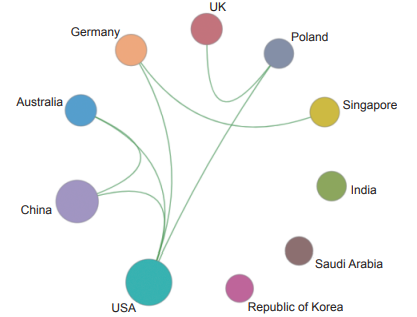
Figure 1.2.1 Collaboration network among major countries in the engineering research front of “theory and technology of large models and their computing systems”
《Table 1.2.2》
Table 1.2.2 Institutions with the greatest output of core papers on “theory and technology of large models and their computing systems”
| No. | Institution | Core papers | Percentage of core papers/% | Citations | Citations per paper | Mean year |
| 1 | Facebook AI Research | 2 | 5.88 | 1 320 | 660 | 2019 |
| 2 | The University of Sydney | 2 | 5.88 | 396 | 198 | 2019 |
| 3 | Harvard University | 2 | 5.88 | 118 | 59 | 2019 |
| 4 | University of Warsaw | 2 | 5.88 | 63 | 31.5 | 2021 |
| 5 | Zhejiang University | 2 | 5.88 | 18 | 9 | 2021.5 |
| 6 | National University of Singapore | 2 | 5.88 | 14 | 7 | 2020 |
| 7 | Huawei Technologies Co., Ltd. | 1 | 2.94 | 346 | 346 | 2021 |
| 8 | Peking University | 1 | 2.94 | 346 | 346 | 2021 |
| 9 | Peng Cheng Laboratory | 1 | 2.94 | 346 | 346 | 2021 |
| 10 | Humboldt University of Berlin | 1 | 2.94 | 113 | 113 | 2017 |
《Figure 1.2.2》

Figure 1.2.2 Collaboration network among major institutions in the engineering research front of “theory and technology of large models and their computing systems”
《Table 1.2.3》
Table 1.2.3 Countries with the greatest output of citing papers on “theory and technology of large models and their computing systems”
| No. | Country | Citing papers | Percentage of citing papers/% | Mean year |
| 1 | China | 1 089 | 44.56 | 2021.4 |
| 2 | USA | 557 | 22.79 | 2021 |
| 3 | Republic of Korea | 142 | 5.81 | 2021.3 |
| 4 | UK | 125 | 5.11 | 2021.2 |
| 5 | Germany | 106 | 4.34 | 2021.1 |
| 6 | Canada | 86 | 3.52 | 2020.9 |
| 7 | Australia | 83 | 3.4 | 2021.3 |
| 8 | India | 79 | 3.23 | 2021.6 |
| 9 | Japan | 76 | 3.11 | 2021.1 |
| 10 | France | 55 | 2.25 | 2021 |
《Table 1.2.4》
Table 1.2.4 Institutions with the greatest output of citing papers on “theory and technology of large models and their computing systems”
| No. | Institution | Citing papers | Percentage of citing papers/% | Mean year |
| 1 | Chinese Academy of Sciences | 103 | 22.01 | 2021.3 |
| 2 | Tsinghua University | 54 | 11.54 | 2021.3 |
| 3 | Peking University | 43 | 9.19 | 2021.3 |
| 4 | Shanghai Jiao Tong University | 42 | 8.97 | 2021.3 |
| 5 | Zhejiang University | 37 | 7.91 | 2021.3 |
| 6 | The Chinese University of Hong Kong | 34 | 7.26 | 2020.5 |
| 7 | Harvard University | 34 | 7.26 | 2020.3 |
| 8 | University of Electronic Science and Technology of China | 33 | 7.05 | 2021.2 |
| 9 | Wuhan University | 33 | 7.05 | 2021.6 |
| 10 | Harbin Institute of Technology | 28 | 5.98 | 2021.7 |
《Figure 1.2.3》

Figure 1.2.3 Roadmap of the engineering research front of “theory and technology of large models and their computing systems”
methods such as reinforcement learning and evolutionary algorithms can be used to automatically design efficient model structures suitable for specific tasks. Therefore, automated neural architecture search and model optimization technologies will be developed in the field of large models in the future. In addition to Huawei’s Pangu, Baidu’s ERNIE Bot, Zhiyuan’s WuDao, and other general-purpose pretraining models, the future will inevitably require more pretraining models for specific fields such as medical care and finance.
Third, privacy and security. With the increasing number of applications based on large models, such as ChatGPT and Dell-E, the privacy of large models has gradually attracted more attention. Future research directions include maintaining high performance of the model while protecting user data privacy. In terms of security, the robustness and fairness of large models will be the focus of future research, including how to make the model perform well on diverse data while avoiding bias against different groups.
Fourth, modeling and reasoning of cross-modal knowledge. Existing technology has enabled the correlation and generation of multimodal data such as images, texts, and audio. However, when faced with more complex and abstract reasoning scenarios, such as protein structure, real-time automatic driving, and multiparty games, existing large models, such as BAI-Chem and Pangu, can only answer questions based on inductive associations in a large amount of training data. To make large models closer to human intelligence, future research will focus on the following: ① quantitative modeling and expression of knowledge in large cross-modal models; ② exploring the relationship between reasoning decisions and knowledge representation in large models; ③ reasonability and interpretability of model multimodal knowledge.
1.2.2 Networking theories and key technologies of satellite internet
Satellite internet is a new revolution in the internet field with global coverage, on-demand access, on-demand service, secure communication, and reliable communication. It provides strong support for the prospect of global interconnection; therefore, it has attracted the interest of many countries. In the 1990s, Motorola Company in the US established the Iridium Satellite System, which consists of 66 low-orbit satellites with inter-satellite links and onboard processing capabilities. Meanwhile, Laura and Qualcomm Companies in the US have built a global satellite system that includes 48 low-orbit satellites, each of which employs transparent forwarding. These two satellite internet systems have undergone bankruptcy restructuring for commercial reasons. After a period of downtime, the satellite internet has recently set off its second craze on an even larger scale. In 2017, the British company OneWeb proposed the OneWeb project, which plans to launch 1 980 satellites to constitute a low-orbit constellation with global coverage. Furthermore, the American company SpaceX plans to launch 42 000 low-orbit satellites to form star links capable of supporting high-speed mobile communication globally. In recent years, China has accelerated the construction of the satellite internet. For example, the “Hongyan Constellation” designed by the China Aerospace Science and Technology Corporation includes 324 satellites, whereas the “Hongyun Constellation” designed by the China Aerospace Science and Industry Corporation includes 156 satellites.
Although satellite internet has grown rapidly, many challenging issues still exist, including network architectures, routing protocols, inter-satellite communication, and mobility management, which are presented as follows.
(1) In terms of network architecture, there are currently two main architectures. The first type is the nonterrestrial network (NTN), which is led by 3GPP, the international organization for the standardization of mobile communication. This open architecture is compatible with existing terrestrial cellular networks and is an integral part of the entire 6G network. The other architecture was specifically designed for the Starlink project by SpaceX Company, which has a closure property. The main research institutions in this area include the Harbin Institute of Technology, the Chinese Academy of Sciences, and Waseda University, Huawei.
(2) In terms of routing protocols, new elastic routing protocols must be developed because satellite networks are highly dynamic, satellite positions constantly vary, and ground network routing protocols are inapplicable. The basic idea is to use the regularity of the constellation motion to map real satellite nodes to virtual nodes. When satellites move or the ground terminal switches, the routing table between virtual nodes is exchanged between physical nodes; thus, the routing information exchange can be completed. The main research institutions in this direction include the University of Surrey, SpaceX, Beijing University of Posts and Telecommunications, Xidian University, the National University of Defense Technology, and Beijing Institute of Technology.
(3) In terms of inter-satellite communication, there are mainly two development trends. The first is inter-satellite microwave communication, which is highly technologically mature and currently has broad applications. However, microwave communication has difficulty meeting the requirements of high-speed communications and has limitations such as limited frequency band capacity and severe co-frequency interference. The second is inter-satellite laser communication, which is widely used in the new- generation satellite internet. Compared with microwave communication, laser communication has several advantages, including large bandwidth, low communication payload, strong anti-interference ability, and good confidentiality. The main research institutions in this direction include the University of Surrey, SpaceX, Chinese Academy of Sciences, Beijing University of Posts and Telecommunications, University of Electronic Science and Technology, and Zhejiang University.
(4) In terms of mobility management, one option is to use centralized mobility management, in which local agents manage terminals. Each time a terminal initiates a location update, the messages are transmitted to local agents. Another option is to use distributed mobility management, in which the Earth is divided into multiple zones, where terminals can register to a virtual gateway composed of satellite clusters covering that zone. Therefore, large-scale satellite network mobility management can be achieved. The main research institutions in this direction include Peng Cheng Laboratory, Southeast University, University of Luxembourg, Huawei, and ZTE Corporation.
Table 1.2.5 shows the main countries that output core papers in this cutting-edge field. China has an obvious advantage, ranking first in the world in terms of the number of core papers with over 67% proportion, and cooperates with Japan, the UK, Saudi Arabia, Republic of Korea, Canada, Australia, and Norway (Figure 1.2.4). The Chinese Academy of Sciences, and Harbin Institute of Technology jointly rank first among the Top 10 institutions that output core papers (Table 1.2.6). Seven institutions are from China, and the rest are from Saudi Arabia, Japan, and Luxembourg. In terms of institutional cooperation (Figure 1.2.5), King Abdulaziz University, Waseda University, and Xi’an University of Posts and Telecommunications have close cooperation. In terms of the number of cited core papers (Table 1.2.7), China still ranks first, with more than 50%, while other countries account for less than 10%. The Top 10 institutions that output cited core papers (Table 1.2.8) were mostly from China, except Waseda University, which ranked sixth, reflecting the strong research strength of China in this field.
Currently, satellite internet is highly valued by major countries and is developing at an unprecedented speed. The development roadmap for this frontier is shown in Figure 1.2.6. The following paragraphs outline its development trends in four areas: network architecture, routing protocols, inter-satellite communication, and mobility management. In terms of network architecture, the NTN architecture is currently in the discussion and standard-setting stage and is expected to be fully developed and commercialized by 2027. In terms of routing protocols, the currently used fixed routing protocols have inherent flaws that seriously constrain the scale and performance of networks, whereas elastic network protocols are gradually improving and are expected to mature by approximately 2026. In terms of inter-satellite communication, microwave communication currently used has low
《Table 1.2.5》
Table 1.2.5 Countries with the greatest output of core papers on “networking theories and key technologies of satellite internet”
| No. | Country | Core papers | Percentage of core papers/% | Citations | Citations per paper | Mean year |
| 1 | China | 21 | 67.74 | 1 097 | 52.24 | 2020.4 |
| 2 | Japan | 4 | 12.9 | 350 | 87.5 | 2020.8 |
| 3 | UK | 4 | 12.9 | 139 | 34.75 | 2021.5 |
| 4 | Saudi Arabia | 3 | 9.68 | 141 | 47 | 2021.3 |
| 5 | Italy | 3 | 9.68 | 119 | 39.67 | 2020.7 |
| 6 | Republic of Korea | 3 | 9.68 | 57 | 19 | 2021 |
| 7 | Canada | 3 | 9.68 | 16 | 5.33 | 2022 |
| 8 | Australia | 2 | 6.45 | 72 | 36 | 2020.5 |
| 9 | Luxembourg | 2 | 6.45 | 49 | 24.5 | 2020 |
| 10 | Norway | 1 | 3.23 | 89 | 89 | 2020 |
《Figure 1.2.4》

Figure 1.2.4 Collaboration network among major countries in the engineering research front of “networking theories and key technologies of satellite internet”
《Table 1.2.6》
Table 1.2.6 Institutions with the greatest output of core papers on “networking theories and key technologies of satellite internet”
| No. | Institution | Core papers | Percentage of core papers/% | Citations | Citations per paper | Mean year |
| 1 | Chinese Academy of Sciences | 3 | 9.68 | 154 | 51.33 | 2019 |
| 2 | Harbin Institute of Technology | 3 | 9.68 | 91 | 30.33 | 2020.3 |
| 3 | King Abdulaziz University | 2 | 6.45 | 137 | 68.5 | 2021 |
| 4 | Waseda University | 2 | 6.45 | 137 | 68.5 | 2021 |
| 5 | Xi’an University of Posts and Telecommunications | 2 | 6.45 | 137 | 68.5 | 2021 |
| 6 | Beijing Institute of Technology | 2 | 6.45 | 102 | 51 | 2021 |
| 7 | Peng Cheng Laboratory | 2 | 6.45 | 87 | 43.5 | 2019.5 |
| 8 | Xidian University | 2 | 6.45 | 71 | 35.5 | 2020.5 |
| 9 | Beijing University of Posts and Telecommunications | 2 | 6.45 | 63 | 31.5 | 2021 |
| 10 | University of Luxembourg | 2 | 6.45 | 49 | 24.5 | 2020 |
《Figure 1.2.5》
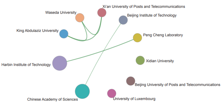
Figure 1.2.5 Collaboration network among major institutions in the engineering research front of “networking theories and key technologies of satellite internet”
《Table 1.2.7》
Table 1.2.7 Countries with the greatest output of citing papers on “networking theories and key technologies of satellite internet”
| No. | Country | Citing papers | Percentage of citing papers/% | Mean year |
| 1 | China | 667 | 51.91 | 2021.3 |
| 2 | Canada | 100 | 7.78 | 2021.5 |
| 3 | USA | 87 | 6.77 | 2021.3 |
| 4 | UK | 77 | 5.99 | 2021.3 |
| 5 | Japan | 67 | 5.21 | 2021.5 |
| 6 | India | 64 | 4.98 | 2021.6 |
| 7 | Republic of Korea | 53 | 4.12 | 2021.7 |
| 8 | Saudi Arabia | 48 | 3.74 | 2021.6 |
| 9 | Australia | 48 | 3.74 | 2021.4 |
| 10 | Italy | 41 | 3.19 | 2021 |
《Table 1.2.8》
Table 1.2.8 Institutions with the greatest output of citing papers on “networking theories and key technologies of satellite internet”
| No. | Institution | Citing papers | Percentage of citing papers/% | Mean year |
| 1 | Harbin Institute of Technology | 70 | 16.09 | 2021.2 |
| 2 | Beijing University of Posts and Telecommunications | 63 | 14.48 | 2021 |
| 3 | Xidian University | 44 | 10.11 | 2021.5 |
| 4 | Peng Cheng Laboratory | 39 | 8.97 | 2021.4 |
| 5 | Chinese Academy of Sciences | 37 | 8.51 | 2021.2 |
| 6 | Waseda University | 34 | 7.82 | 2021.6 |
| 7 | Southeast University | 32 | 7.36 | 2021.2 |
| 8 | Beijing Institute of Technology | 30 | 6.9 | 2021.6 |
| 9 | National University of Defense Technology | 30 | 6.9 | 2021.1 |
| 10 | University of Electronic Science and Technology of China | 29 | 6.67 | 2021.4 |
《Figure 1.2.6》

Figure 1.2.6 Roadmap of the engineering research front of “networking theories and key technologies of satellite internet”
communication rates and strong interference and is gradually being replaced by inter-satellite laser communication, which is expected to be completed by 2026. In terms of mobility management, the existing centralized management is transitioning to distributed management because of its high signaling overhead and transmission latency. The development trend of satellite internet is summarized as follows. First, the satellite internet has shifted from focusing on communication to integrating communication, navigation, and remote sensing, allowing for a multifunctional satellite internet. Second, satellite internet has developed from ground-devices-assisted access to mobile satellite communication without a ground station, achieving the goal of on-demand access. Third, has developed from satellite internet to satellite IoT to achieve the vision of the interconnection of all things. In terms of the application scenarios of satellite internet, has been used in emergency communication, remote area communication, and logistic communication. With the rapid development of the satellite internet, it will be widely used in various fields such as the economy, society, and military in the future.
1.2.3 Ultra-large-scale silicon-based quantum chips
A quantum chip is a device designed and manufactured based on the principles of quantum mechanics for applications in quantum computing and communications. Unlike classical chips, which use binary bits, quantum chips use quantum bits (qubits) as their fundamental information units. Qubits can exist in superpositions 0 and 1, and they can share information among multiple qubits through entanglement. This characteristic endows quantum chips with significant advantages in addressing specific problems, allowing them to solve certain computationally challenging tasks, such as large-integer factorization, quantum simulation, and optimization, at faster speeds than classical computers. Fabricating and manipulating quantum chips are a challenging because of the fragility of quantum bits, which are susceptible to destruction by uncontrollable environmental influences. A universal quantum computer often requires a substantial number of qubits to implement a quantum error correction and achieve the desired quantum advantage. Nevertheless, in terms of the number of qubits alone, various physical implementations, including superconducting circuits, diamond nitrogen-vacancy centers, and trapped ion technologies, are yet to meet these demands. Consequently, the production of large-scale quantum chips containing millions of qubits has emerged as a critical challenge for the realization of universal quantum computing. Given the successful manufacture of chips containing billions of transistors within the traditional semiconductor industry, the integration of silicon-based electronics with quantum technology holds the promise of establishing a quantum computing platform for the existing semiconductor manufacturing infrastructure. The compatibility of silicon-based quantum chips with traditional semiconductor processes provides advantages in terms of production cost, scalability, and integration. This has propelled large-scale silicon-based quantum chips into a focal point of research in the field of quantum computing, offering a promising pathway for the feasibility and scalability of quantum computing.
Silicon-based quantum chips present various development routes. One approach involves encoding quantum information into electron (hole) spins confined in gate-defined silicon quantum dots or implanted phosphorus nuclear spins embedded in silicon. In 1998, theoretical physicists predicted that spin states within silicon nanostructures could serve as carriers of quantum information, marking the inception of an experimental research race. Single-qubit operations can be achieved by manipulating and measuring the individual electron spins. Leveraging the exchange interaction between the two spins enables the implementation of two-qubit gate operations. Initial experiments used III–V semiconductor materials; however, unavoidable hyperfine interactions hindered their further advancement. In 2013, several research groups simultaneously reported breakthroughs in silicon-based spin qubits. This was facilitated by the isotopic purification of silicon to suppress hyperfine interactions, resulting in a significant enhancement in fidelity. Currently, single-qubit and two-qubit gates with fidelity far exceeding the error-correction thresholds have been realized. Furthermore, because of the nanoscale physical dimensions of silicon quantum dots and dopant atoms and their compatibility with modern IC technology, they can be scaled up to large-scale qubit arrays with reasonable chip footprints. Quantum processors comprising six qubits have already been demonstrated as larger quantum dot platforms in one-dimensional and two-dimensional configurations.
Another approach is to use silicon-based photonic integration processes to achieve quantum entanglement between photons and quantum-state manipulation, thereby enabling quantum computing and communications. Photonic quantum technology stands out because of its advantages, such as longer decoherence time, multiple degrees of freedom, no need for vacuum, and low temperature. In contrast to the bulky, unstable, and poorly scalable traditional optical instruments, silicon-based photonic chips fabricated using CMOS nanomanufacturing techniques offer high integration, stability, controllability, and scalability. Currently, integration of several hundred optical components on a single chip has been achieved, and it is expected that various core photonic quantum functionalities, including quantum light sources, quantum control pathways, and single-photon detectors, can be integrated on a single chip. In recent years, silicon-based photonic chips achieved made significant breakthroughs in the fields of boson sampling, multiphoton high-dimensional quantum entangled states, quantum key distribution, and quantum teleportation.
In recent years, there have been numerous significant achievements in the field of large-scale silicon-based quantum chips. The countries and institutions contributing to the key research papers are outlined in Tables 1.2.9 and 1.2.10. The USA, the UK, and Netherlands rank among the top three nations in terms of the number of key research papers published. Prominent contributing institutions include Delft University of Technology, University of Bristol, and Peking University. Furthermore, many of these key research papers resulted from collaborations between various research institutions across different countries, as illustrated by the collaboration networks between leading countries and institutions in Figures 1.2.7 and 1.2.8. Tables 1.2.11 and 1.2.12 list the main countries and institutions responsible for citing key papers in this field. The Chinese Academy of Sciences and University of Science and Technology of China rank the top two, reflecting China’s notable interest and engagement in this direction.
From the perspective of the overall development trajectory within the field, ultra-large-scale silicon-based quantum chips are still in their nascent stages and many key problems must be solved. As depicted in Figure 1.2.9, future development of ultra-large-scale silicon-based quantum chips will focus on the following key directions:
(1) Silicon-based spin quantum chips
1) Large-scale arrays: The practical realization of spin quantum chips requires increasing the fidelity of the initialization, manipulation, and readout modules for each qubit to sufficiently high levels. Large-scale fabrication of high-fidelity qubits using CMOS technology is difficult because the properties of spin qubits, such as valley splitting, spin-orbit coupling, and tunneling coupling between quantum dots, are very sensitive to atomic-level defects. Therefore, the quality of the material growth is crucial. Rapid detection and automated control of each qubit’s parameters are also essential.
2) Long-range coupling: Currently, most silicon-based spin qubits rely on nearest-neighbor coupling, which requires proximity between quantum dots or phosphorus-doped atoms, limiting the layout of the dense arrays. Developing methods for long-range coupling can enable the separation of qubits to over larger distances. Several experimental approaches have been explored, including floating gates, microwave cavities, superconducting resonators, and electron shuttling.
《Table 1.2.9》
Table 1.2.9 Countries with the greatest output of core papers on “ultra-large-scale silicon-based quantum chips”
| No. | Country | Core papers | Percentage of core papers/% | Citations | Citations per paper | Mean year |
| 1 | USA | 24 | 42.86 | 3059 | 127.46 | 2019.7 |
| 2 | UK | 15 | 26.79 | 2436 | 162.4 | 2018.7 |
| 3 | Netherlands | 13 | 23.21 | 2135 | 164.23 | 2019.5 |
| 4 | Australia | 12 | 21.43 | 1441 | 120.08 | 2019.7 |
| 5 | China | 11 | 19.64 | 1603 | 145.73 | 2019.5 |
| 6 | Japan | 11 | 19.64 | 1075 | 97.73 | 2020.1 |
| 7 | Germany | 9 | 16.07 | 1621 | 180.11 | 2019.8 |
| 8 | Denmark | 6 | 10.71 | 748 | 124.67 | 2020.3 |
| 9 | Republic of Korea | 4 | 7.14 | 542 | 135.5 | 2019.5 |
| 10 | Switzerland | 4 | 7.14 | 226 | 56.5 | 2021.2 |
《Table 1.2.10》
Table 1.2.10 Institutions with the greatest output of core papers on “ultra-large-scale silicon-based quantum chips”
| No. | Institution | Core papers | Percentage of core papers/% | Citations | Citations per paper | Mean year |
| 1 | Delft University of Technology | 11 | 19.64 | 1 940 | 176.36 | 2019.5 |
| 2 | University of Bristol | 9 | 16.07 | 1 319 | 146.56 | 2018.6 |
| 3 | Peking University | 6 | 10.71 | 753 | 125.5 | 2020.2 |
| 4 | Technical University of Denmark | 6 | 10.71 | 748 | 124.67 | 2020.3 |
| 5 | Netherlands Organization for Applied Scientific Research | 6 | 10.71 | 577 | 96.17 | 2020 |
| 6 | QuTech | 5 | 8.93 | 493 | 98.6 | 2019.8 |
| 7 | The University of New South Wales | 5 | 8.93 | 492 | 98.4 | 2019.6 |
| 8 | University of Stuttgart | 4 | 7.14 | 902 | 225.5 | 2020 |
| 9 | Heriot-Watt University | 4 | 7.14 | 741 | 185.25 | 2019 |
| 10 | University of Electronic Science and Technology of China | 4 | 7.14 | 693 | 173.25 | 2018.5 |
《Figure 1.2.7》

Figure 1.2.7 Collaboration network among major countries in the engineering research front of “ultra-large-scale silicon-based quantum chips”
《Figure 1.2.8》

Figure 1.2.8 Collaboration network among major institutions in the engineering research front of “ultra-large-scale silicon-based quantum chips”
《Table 1.2.11》
Table 1.2.11 Countries with the greatest output of citing papers on “ultra-large-scale silicon-based quantum chips”
| No. | Country | Citing papers | Percentage of citing papers/% | Mean year |
| 1 | USA | 1 281 | 23.69 | 2020.6 |
| 2 | China | 1 157 | 21.4 | 2020.8 |
| 3 | Germany | 558 | 10.32 | 2020.7 |
| 4 | UK | 461 | 8.53 | 2020.4 |
| 5 | Australia | 412 | 7.62 | 2020.4 |
| 6 | Japan | 325 | 6.01 | 2020.6 |
| 7 | Canada | 302 | 5.59 | 2020.4 |
| 8 | France | 273 | 5.05 | 2020.5 |
| 9 | Italy | 232 | 4.29 | 2020.6 |
| 10 | Netherlands | 207 | 3.83 | 2020.5 |
《Table 1.2.12》
Table 1.2.12 Institutions with the greatest output of citing papers on “ultra-large-scale silicon-based quantum chips”
| No. | Institution | Citing papers | Percentage of citing papers/% | Mean year |
| 1 | Chinese Academy of Sciences | 225 | 16.78 | 2020.6 |
| 2 | University of Science and Technology of China | 213 | 15.88 | 2020.7 |
| 3 | Delft University of Technology | 145 | 10.81 | 2020.4 |
| 4 | The University of New South Wales | 112 | 8.35 | 2020.5 |
| 5 | Massachusetts Institute of Technology | 111 | 8.28 | 2020.6 |
| 6 | Harvard University | 103 | 7.68 | 2020.2 |
| 7 | University of Technology Sydney | 93 | 6.94 | 2020.6 |
| 8 | Université Grenoble Alpes | 89 | 6.64 | 2020.8 |
| 9 | University of Bristol | 85 | 6.34 | 2019.9 |
| 10 | The University of Maryland | 84 | 6.26 | 2020.4 |
《Figure 1.2.9》

Figure 1.2.9 Roadmap of the engineering research front of “ultra-large-scale silicon-based quantum chips”
(2) Silicon-based integrated photonic quantum chips
1) Large-scale integration: Integrating quantum light sources, quantum-state manipulation pathways, and single-photon detectors on a single chip while meeting all the key performance metrics remains a challenge. It is critical to reduce the losses caused by the interaction between photons and the surrounding medium within the chip. In addition, to realize practical applications, the complexity of the multiphoton high-dimensional entangled states that photonic quantum chips can generate must be continuously improved to achieve a sufficiently large state space.
2) Multichip interconnects: As the number of qubits increases, it becomes increasingly difficult to integrate more optical components on a single chip. Future developments may leverage the advantages of optical communication to achieve interconnectivity between multiple chips, thereby enabling the construction of large-scale quantum processors through distributed quantum computing. However, achieving high performance interconnects between silicon-based integrated photonic quantum chips remains a technical challenge, thereby necessitating the development of ultralow-loss interconnect technologies to enhance the fidelity of quantum-state transmission between chips.
Ultra-large-scale silicon-based quantum chips have tremendous potential in various applications. Both silicon-based spin quantum chips and silicon-based integrated photonic quantum chips are poised to become pivotal components of future quantum technologies, with profound implications for solving complex problems and enhancing information security. In the future, silicon- based quantum chips will continue to progress toward greater scalability and broader applications owing to their compatibility with traditional CMOS technology.
《2 Engineering development fronts》
2 Engineering development fronts
《2.1 Trends in Top 10 engineering development fronts》
2.1 Trends in Top 10 engineering development fronts
The Top 10 engineering development fronts in the information and electronic engineering field are summarized in Table 2.1.1, encompassing the subfields of electronic science and technology, optical engineering and technology, instrument science and technology, information and communication engineering, computer science and technology, and control science. “Light-controlled phased-array technology”, “control technology of unmanned systems based on brain–computer interface”, and “artificial- intelligence-based fault diagnosis and detection” are fronts of data mining. The remaining fronts of expert nomination. The annual number of core patents published for the Top 10 engineering development fronts from 2017 to 2022 is listed in Table 2.1.2.
(1) Light-controlled phased-array technology
A light-controlled phased-array antenna (LCPAA) mainly includes transmitting-receiving (TR) modules, an antenna array, light- sensitive components, and a light-controlling module, in which the radiation characteristics of the LCPAA are engineered by manipulating the electromagnetic response of light-sensitive materials (and/or components) in the space-/time-/frequency-/ spectrum-domains through light. Without loss of generality, the controlling parameters can be the intensity, wavelength, beam
《Table 2.1.1》
Table 2.1.1 Top 10 engineering development fronts in information and electronic engineering
| No. | Engineering development front | Published patents | Citations | Citations per patent | Mean year |
| 1 | Light-controlled phased-array technology | 260 | 1 063 | 4.09 | 2020 |
| 2 | Control technology of unmanned systems based on brain–computer interface | 464 | 1 344 | 2.9 | 2019.8 |
| 3 | Computing power network construction technology for diverse computing | 638 | 3 034 | 4.76 | 2019.9 |
| 4 | Flexible intelligent tactile sensor | 616 | 5 105 | 8.29 | 2019.1 |
| 5 | High-speed free-space optical communication technology | 1 018 | 2 061 | 2.02 | 2020.1 |
| 6 | Terahertz solid-state phased-array integrated circuit | 887 | 2 022 | 2.28 | 2019.9 |
| 7 | Artificial-intelligence-based fault diagnosis and detection | 991 | 5 736 | 5.79 | 2020.9 |
| 8 | Large-size silicon carbide materials and power chips | 232 | 366 | 1.58 | 2020.1 |
| 9 | Naked eye 3D technology based on light-field technology | 668 | 3 379 | 5.06 | 2019 |
| 10 | Augmented reality space operating system | 420 | 1 949 | 4.64 | 2019.9 |
《Table 2.1.2》
Table 2.1.2 Annual number of core patents published for the Top 10 engineering development fronts in information and electronic engineering
| NO. | Engineering development front | 2017 | 2018 | 2019 | 2020 | 2021 | 2022 |
| 1 | Light-controlled phased-array technology | 25 | 37 | 46 | 42 | 39 | 71 |
| 2 | Control technology of unmanned systems based on brain–computer interface | 58 | 78 | 73 | 67 | 88 | 100 |
| 3 | Computing power network construction technology for diverse computing | 77 | 77 | 109 | 125 | 101 | 149 |
| 4 | Flexible intelligent tactile sensor | 127 | 136 | 96 | 107 | 82 | 68 |
| 5 | High-speed free-space optical communication technology | 115 | 138 | 127 | 128 | 214 | 296 |
| 6 | Terahertz solid-state phased-array integrated circuit | 94 | 112 | 162 | 133 | 176 | 210 |
| 7 | Artificial-intelligence-based fault diagnosis and detection | 18 | 38 | 99 | 151 | 293 | 392 |
| 8 | Large-size silicon carbide materials and power chips | 26 | 27 | 21 | 43 | 46 | 69 |
| 9 | Naked eye 3D technology based on light-field technology | 168 | 154 | 106 | 89 | 75 | 76 |
| 10 | Augmented reality space operating system | 47 | 61 | 72 | 63 | 79 | 98 |
direction, time light delay, or a combination of these. The LCPAA has been widely used in wireless communication, remote sensing, positioning, precision detection, and other applications. Depending on the frequency at which the radiation occurs, LCPAA technology mainly involves two categories: ① optical phased-array (OPA) for optical communication and optical sensing (such as laser radars), which is also known as space-light modulation; ② microwave-optical phased array for microwave communication, detection, and sensing (such as microwave radars). Low cost, high efficiency, wide angular view, large bandwidth, and high space-time resolution are highly desirable characteristics of the two types of LCPAAs.
To clarify, the microwave-optical phased array has two subcategories: ① microwave-photonic phased arrays (MPPA) and ② optically tuned microwave phased arrays (OTMPA). The MPPA uses time-delay light as a microwave carrier for wideband low-loss microwave transmission, but it faces challenges such as the compact integration of a light–microwave converter, precision time-delay of optical waveguides, scalable microwave-photonic transmission modules, and a compact yet high-power laser source. However, OTMPA addresses the critical challenges of achieving multipolarized high gain at high frequency using light- induced microwave modulation, thereby eliminating the need for complex feeding networks and high-cost precision fabrication in conventional electrically tuned phased arrays. Further improvement in the performance of OTMPAs requires high-speed optical- microwave switches, high-contrast light-sensitive materials, and innovative architecture design for high-precision control of the microwave phase by light. On the optical radiation side, the current research trend of OPA mainly focuses on the development of light delay and light-modulators for multiple-light-beamforming, where various light-modulation mechanisms have been proposed, such as heat, mechanical, electrical, liquid–crystal, and phase-changing modulations.
(2) Control technology of unmanned systems based on brain–computer interface
The brain–computer interface-based control technology of the unmanned system combines neurobiology, informatics, AI, and unmanned systems to collect and analyze physiological signals generated by brain activity. It decodes human brain intentions and converts them into control commands, which are then encoded to enable interaction and control between the human brain and the unmanned systems. With this technology, users can directly control unmanned systems using physiological signals, such as electroencephalography (EEG), without the need for traditional human–computer interaction.
The main technical directions are as follows:
1) Acquisition and transmission of brain signals: Different types of biosensors (such as electroencephalographs and eye trackers) are used to capture physiological information from the human brain. The signals are amplified and converted into digital signals.
2) Processing and decoding of brain signals: To identify feature patterns in brain signals and decode human brain intentions, complex and high-dimensional brain activity data are processed using signal processing methods such as noise reduction and feature extraction.
3) Commands generation and control of unmanned systems: The identified feature patterns of human brain intentions are converted into corresponding control commands using encoding techniques. These commands are used to control unmanned systems such as drones, autonomous vehicles, robots, and exoskeletons. In addition, it is important to ensure the comfort, convenience, stability, and real-time nature of human–computer interaction.
Traditional unmanned systems based on AI have limitations in responding to some abnormal states that are of low probability. To address this issue, the integration of the brain–computer interface (BCI) into unmanned systems leverages the fusion of brain– computer intelligence, fully leveraging the advantages of human and computer intelligence. This approach opens a new avenue for enhancing the intelligence of unmanned systems. It is expected to have broad application prospects in fields such as aviation, aerospace, navigation, autonomous driving, traffic safety, elderly and disability assistance, medical support, rescue operations, industrial control, education, and entertainment.
(3) Computing power network construction technology for diverse computing
Computing power networks are technical concepts that connect cross-center computing power through networks. They rely on high-speed, mobile, secure, and ubiquitous network connections that integrate multilevel computing resources, such as the net, cloud, number, intelligence, security, edge, end, and chain. China was the first country to propose this new type of integrated basic service that combines data sensing, transmission, storage, and computing. Its goal is to integrate multilevel computing resources and build a new infrastructure system centered on computing and networking. Computing power network construction technology for diverse computing refers to the use of high-performance and cloud computing, high-performance networks, distributed storage, and other technical means to effectively integrate and schedule heterogeneous computing resources and provide users with flexible, efficient, and scalable computing, storage, network, application, and data services. This technology meets the demands for diversity and dynamism of computing resources in different application scenarios to support complex computing tasks in AI, big data analysis, virtual reality, and other fields.
The main technical directions include heterogeneous resource integration and collaboration, computing resource and service encapsulation, intelligent task scheduling, and dynamic metering and billing. Heterogeneous resource integration and collaboration connect heterogeneous and network computer resources through unified interfaces and protocols to form a unified computing resource pool and provide users with a flexible and scalable computing environment. Computing resources and service encapsulation describe, encapsulate, and invoke the underlying cloud platform resources. Intelligent task scheduling designs reasonable scheduling algorithms and load-balancing strategies based on the characteristics of tasks and hardware platforms and automatically selects the optimal execution environment and resource configuration. Dynamic metering and billing ensure accurate metering and standardized billing for the resource usage of combined clusters across management domains.
With the development of AI, computing power network construction technology will become more intelligent, automatically selecting the optimal combination of computing resources and allocation strategies based on factors such as task type, resource characteristics, and user demand. Future development will focus on data privacy protection, network security protection, and fault-tolerance mechanism design to ensure the stable operation of the computing resource network and security of user data. With the popularity of 5G technology and the development of edge computing, a computing power network for diverse computing will achieve closer integration with 5G networks and edge devices, and provide users with faster, real-time responsive computing services using their computing power and low-latency characteristics.
(4) Flexible intelligent tactile sensor
The tactile sensor, as a key support technology for robots, is a bridge that connects the external environment and robot body to imitate the tactile sensing ability of human skin and realize the robot’s sensitive and accurate perception of the physical information of the external environment. Flexible intelligent tactile sensors combine flexible electronic technology and intelligent perception algorithms with measurement adaptability and contact information intelligence, thereby allowing robots to perform intelligent interaction and manipulation tasks on complex robot bodies and object surfaces in nonstructural environments.
At present, its main technical directions include ① flexible material and its manufacturing technology, ② perception mechanism and algorithm, ③ tactile sensing simulation, and ④ multimodal perception integration and application in manipulation.
First, new flexible polymers, nanomaterials, and biomaterials with good electrical and mechanical properties must be used to fabricate substrate, sensing layer, and electrode materials for flexible tactile sensors to enhance their flexibility, durability, and adaptability. In addition, generalized intelligent sensing methods have been developed to enable sensors to achieve sensitive and accurate sensing of multimodal parameters, such as contact force, shape, temperature, and position. To cope with the high cost of obtaining large-scale data for tactile sensors, it is critical to develop high-quality tactile sensing simulation platforms and the corresponding migration algorithms. Tacchi, a representative visual-based tactile sensor simulator, can provide rich tactile information and improve tactile learning efficiency. It also combines various flexible tactile sensing mechanisms and large neural networks to achieve multimodal sensory fusion of sensors, leading to a more comprehensive and in-depth understanding of the environment and providing more complete, diverse, and accurate tactile sensory feedback, which is then applied to sophisticated manipulation tasks and achieving the bioinspired process from tactile perception to operation.
(5) High-speed free-space optical communication technology
High-speed free-space optical communication technology uses laser beams as carriers for high-speed information transmission in free-space. Compared to traditional microwave communication, it has advantages such as high speed (up to 100 Gb/s), strong resistance to electromagnetic interference, and no spectrum restrictions. In addition, it has the benefits of a small terminal size, lightweight, low-power consumption, and easy deployment. Based on these features, high-speed free-space optical communication technology has significant strategic and practical applications in the military and civilian domains, including planetary exploration, lunar exploration, Earth observation, navigation reconnaissance, low-Earth-orbit mobile communication, and emergency rescue.
However, because of the long traveling distance of the laser in space, it is prone to divergence, and several factors, such as atmospheric absorption, refraction, background light interference, and cloud particle scattering, may adversely affect ground reception. Therefore, high-power light sources, high-spectral efficiency modulation, high-sensitivity interference-resistant optical signal reception, precise and reliable high gain antenna design, fast and accurate acquisition, pointing, and tracking technology, and dynamic and robust optical networking technology are just a few of the challenges that technology still faces in implementing a high-speed, stable, reliable, and cost effective optical space information networks.
In recent years, some countries have preliminarily acquired the capability of 100 Gb/s space laser communication because of the global deployment of space information networks and relentless exploration of high-power semiconductor lasers, precise optical filtering devices, highly sensitive optical detectors, and rapid, precise integrated optomechatronic technology. Currently, space optical communication technology is gradually shifting from a point-to-point mode to relay forwarding and the establishment of high-speed, intelligent, and integrated optical space information networks.
(6) Terahertz solid-state phased-array integrated circuit
Terahertz solid-state phased-array integrated circuit (IC) can steer the beam direction flexibly, implement fast tracking, and precisely detect targets in terahertz communication and radar imaging systems through highly integrated transceiver, switching, and amplitude-phase control devices, significantly reducing the system volume and cost. Terahertz waves are electromagnetic waves with a frequency range of 100 GHz to 10 THz. Their electromagnetic spectrum is between the microwave frequency band and the infrared spectrum, and is in a special position between the traditional electronics and photonics research frequency bands, with large communication transmission capacity, high resolution, good penetration, and excellent spectral characteristics. Because of the widespread installation of cellular communication and wireless sensing, the spectrum resources below 30 GHz are already crowded, and it is highly desirable to develop a spectrum resource in the terahertz band. However, because of the large propagation loss in the terahertz band and limited device power, it is necessary to use phased-array systems to provide high antenna gain and dynamic beam tracking. Therefore, terahertz solid-state phased-array ICs based on advanced compounds and silicon-based IC processes are the core technical solution of terahertz technology, and have become the focus of research in the emerging generation of wireless communication and high-precision terahertz radar systems.
In recent years, the cut-off operating frequency and device performance of silicon-based terahertz IC technology have increased rapidly because of the continuous improvement in compound- and silicon-based IC processes, particularly driven by Moore’s law. Terahertz solid-state phased-array IC technology significantly improves the performance and reliability of terahertz systems by improving system integration and reducing the physical size of the system, while also reducing system cost and application technical requirements. Terahertz solid-state phased IC technology has become an important strategic direction in the field of electronic information. In 2021, the USA Defense Advanced Research Projects Agency (DARPA) launched the “G-band Array Electronics” (ELGAR) project, and China has also supported and financed similar research projects in this field. In the future, terahertz solid-state phased-array IC technology will be further developed for higher frequencies, higher integration, and better performance.
(7) Artificial-intelligence-based fault diagnosis and detection
AI-based fault diagnosis and detection processes data uses machine learning techniques (e.g., deep neural networks) to achieve fault detection, diagnosis, and prediction of test objects. In recent years, research on AI-based fault diagnosis and detection has received extensive attention globally. The main directions include: ① generalized intelligent fault diagnosis and detection, adaptability in complex environments, and transferability across different scenarios; ② interpretable intelligent fault diagnosis and detection, such as constructing interpretable network models and visualizing the semantic information embedded in features; ③ intelligent fault diagnosis and detection with weak data quality, such as exploring generative models for data complementation, and meta-learning-based diagnosis and detection algorithms; ④ information fusion-based intelligent fault diagnosis and detection, including data-, feature-, and decision-level fusion; ⑤ lightweight intelligent fault diagnosis and detection, such as deep neural network compression and intelligent models for edge and mobile devices.
Despite the plethora of AI-based fault diagnosis and detection methods, several key bottlenecks remain rarely addressed, including: ① significant data dependency and lack of mechanism analysis during data mining processes; ② insufficient research on boundaries and factors influencing model generalization; ③ lack of research on the mechanism and quantitative standards for interpretability; ④ credibility concerns underlying the deployment of AI models in risk-sensitive scenarios. Based on the aforementioned issues, accelerating the advancement of intelligent fault diagnosis and detection technology in areas such as technological innovation, engineering practices, and trustworthy safety will be an important direction for the future development of fault diagnosis and detection technology based on AI.
(8) Large-size silicon carbide materials and power chips
Large-size silicon carbide (SiC) materials are mainly SiC single-crystal substrates with a diameter of 6 inches (150 mm) or even larger. They are used to obtain high-quality epitaxial films for the fabrication of high-performance power chips. Large-scale deployment of semiconductor SiC materials and chips is emerging, targeting the goals of carbon peaking and carbon neutrality. As an IV-IV compound semiconductor material, SiC has a wide bandgap, high thermal conductivity, high breakdown field strength, high electron saturation drift rate, and excellent chemical and thermal stabilities. SiC is expected to be widely used in the field of power electronics related to renewable energy due to the fact that SiC power devices can work at higher temperature, higher breakdown voltage and faster switching speed, lower on-resistance, and better durability compared with silicon power devices.
For large-size SiC materials, the main direction of technological innovation is to increase the size and thickness of SiC single crystal and reduce the defect density of SiC single crystal, enabling lower-cost and higher-quality SiC substrates. The size of SiC single crystal has increased over the years. The mainstream SiC substrate size is now 6 inches. Research institutions and companies are competing to develop technologies for 8-inch SiC single crystal and substrates. The thickness of a SiC single crystal is typically in the range of 10–30 mm. There is still a long way to go in the development of meter-long SiC single-crystal-like silicon single crystal. For SiC single crystal volume defects, such as micropipes have been almost eliminated. However, the density of other defects, such as dislocations, remains high, generally on the order of magnitude of 103/cm2, which needs to be significantly reduced.
SiC diodes have been well developed. In contrast, the performance of SiC metal-oxide-semiconductor field effect transistors (MOSFETs) needs to be improved. First, the activation of implanted ions in the injection region of MOSFETs should be improved, which critically depends on ion implantation and subsequent high-temperature annealing during device fabrication. Second, optimizing the key parameters for thermal oxidation and annealing to reduce the density of interface defects and oxide defects is an important issue that should be addressed to enhance the electron mobility and gate-oxide reliability of MOSFETs. Finally, the reliability of MOSFETs must be significantly improved in terms of gate-oxide growth and post-annealing techniques, short-circuit robustness, anti-surge and anti-avalanche, and irradiation reinforcement.
(9) Naked eye 3D technology based on light-field technology
Naked eye three-dimensional (3D) technology based on light-field technology refers to a technology that uses light tracing to construct 3D objects by reproducing elements such as the luminous position in the all-light equation, two luminous angles of the direction of the observation position, wavelength of light λ , and the observation time t, thereby allowing users to directly see “3D objects in the real world” through their eyes. Compared with traditional naked eye 3D display technology, the light-field display increases the displacement parallax based on binocular parallax to have ultra-high information density and spatial bandwidth, providing the user with a retinal-level visual experience.
The concept of the light field was proposed in 1936, and it can be divided into two parts: light-field acquisition (imaging) and light-field display. Light-field acquisition includes camera arrays, microlens arrays, and pinhole imaging. The light-field display includes Magic Leap’s scanning type, multiprojection type, Stanford University’s multilayer screen technology, Ricoh’s multifocal surface, and integrated imaging technology implementation types. The scanning type uses a high-speed projector and a rotating directional scattering screen to produce a horizontal multiview; however, its equipment and site requirements are strict. The multiprojection type uses a projection array and a rotating/directional scattering screen to generate a horizontal multiview. Its equipment size and cost are limited. The multilayer screen type uses a multilayer LCD screen and directional backlight or ordinary backlight, with the algorithm to achieve a continuous depth-of-field. The current technical bottleneck is focused on algorithm research. A multifocal surface LCD screen or microdisplay with microlevel zoom lens design could achieve a continuous depth-of- field with the support of certain algorithms. In addition, the optimal combination between different algorithms is also the most concerned research content for this field, in order to achieve an ideal continuous depth-of-field finally. Integrated imaging uses a panel and lens array to achieve a continuous depth-of-field, and a light-field camera to obtain the video source and then reproduce it by the array lens.
By using light-field display technology to reconstruct the light-field distribution of 3D objects in space, a 3D display effect that is close to the natural world can be realized. Therefore, in the future, naked eye 3D technology based on light-field display will be an important information interaction mode. Ultra-high resolution display panels, which benefit from the continuous development of semiconductor display technology, expand the possibilities for optical field naked eye 3D display technology. Combined with eye tracking and motion capture, intelligent interaction under pupillary-level dense viewing points will be realized gradually.
The advancement of display technology will promote the advancement of the entire industrial chain, including display chips, high-resolution panel materials, 3D content, and the development of upstream and downstream ecological linkages. With the gradual improvement of the industrial chain, the naked eye 3D display based on light-field technology will soon achieve industrial application breakthroughs in medical imaging, detection, and minimally invasive surgery. Additionally, it will enable electronic industry design automation, online education model innovation, commercial exhibition display, culture, and entertainment.
(10) Augmented reality space operating system
The augmented reality space operating system is a 3D operating system designed for extended reality (XR) devices that enable the interplay of virtual and real-time interactions and realistic presentations. The primary objective is to weave a virtual space into the fabric of the real world using spatial perception technology. It supports 3D multimodal user interactions via recognition algorithms, such as eye tracking and gestures, to construct a spatial application system that enables natural interactions, thereby realizing multichannel, natural interactive operations within an immersive virtual-reality fusion space. Unlike traditional PC and mobile operating systems, the augmented reality space operating system underscores the user’s immersive experience in 3D space. This enables users to append virtual objects to the physical world, thereby enriching the blend of virtual and real presentations and interactions. The spatial operating system, compared to screen interfaces, promotes more natural and intuitive operations and interactions, forming the cornerstone of the meta-universe application ecosystem.
The research directions include the followings. ① Spatial application system: We should construct and manage spatial applications running on XR devices by leveraging the high-performance 3D rendering engine at the system level. This involves defining a new 3D application system and exploring the most effective ways to design, render, and use 3D applications in space. ② Spatial interaction system: Based on a human-centered design concept, we should research and develop a natural, intuitive, and efficient user interaction mode based on the multimodal interactions of multiple recognition algorithms. ③ Spatial perception fusion: We should develop efficient algorithms for spatial positioning, tracking, and environmental understanding, enabling XR devices to better perceive their environment and achieve the seamless integration of virtual content and physical space.
In the future, the augmented reality space operating system may revolutionize the traditional operating system model with a new spatial application system. Innovative interaction methods, such as eye tracking and gestures, can provide a more realistic and natural human-machine interface, spatial understanding, perception capabilities, and stronger interactive applications. The final goal is to achieve efficient acquisition and processing of hybrid and enhanced intelligent information, resulting in experiences that transcend the real space.
《2.2 Interpretations for three key engineering development fronts》
2.2 Interpretations for three key engineering development fronts
2.2.1 Light-controlled phased-array technology
Since the 1890s, phased-array technology has been widely used in wireless communication, remote sensing, security checks, medical instruments, and imaging systems for both defense and civil applications. As the 21st century witnessed the rapid growth of the big data market due to the development of 5G/6G mobile networks, IoT, and AI, “optical transmission” started to replace “electrical transmission” to achieve higher data transmission rates, from which the development of light-modulator, light-switches, and optical waveguides greatly benefit the application of “optical-modulation concept” in microwave phased arrays to cater for the demand of low-cost high-performance phased arrays, such as the aforementioned MPPA and OTMPA.
MPPA focuses on the wideband low-cost transmission of phased microwave signal using light as the carrier, thereby improving the scanning range and bandwidth of phased arrays by greatly reducing the heat emission and transmission loss caused by large-scale microwave feeding networks and TR modules in conventional phased arrays. Meanwhile, MPPA is advantageous in its native anti-radiation characteristic because of the different frequencies used for transmitting/receiving and wave guiding, which is particularly useful in space applications. A recent technological trend is the development of highly integrated on- chip microwave-photonic modulators with higher precision, dynamic range, scale time delay, and resolution to improve the scanning ability of phased arrays. Representative research institutes in this technology include Zhejiang University, Tsinghua University, University of Electronic Science and Technology of China, China Electronics Technology Group Corporation, University of Ottawa, University College London, USA Naval Research Laboratory, University of Virginia, University of California, and Osaka University.
OTMPA focuses on the use of light-sensitive materials or components to tune the amplitude/phase distribution over the antenna aperture and waveguide structures through controllable light rather than a conductive medium such as conductive wires, which significantly reduces the ohmic loss and surface-wave loss caused by massive complex passive microwave feeding networks and the power loss caused by conventional active-phase shifters. Consequently, the optical-tuning microwave radiation principle offers higher gain (owing to scalability), antenna efficiency (owing to simpler feeding), operating frequency (owing to lower ohmic loss of wave-guiding structures), and degrees of freedom in polarization (owing to wireless optical tuning). Representative research institutes in this technology include: ① Australian National University, which first proposed the concept and validation of light- controlled metamaterials in 2012 by combining photonic diodes and varactors; ② USA Naval Research Laboratory, which patented the use of light-sensitive films for 1-bit optically tuned reflectarray antennas in 2020; ③ Southeast University and Xidian University, which combine photon cells and varactors/phototon-resistors for optically tuned reflective metasurfaces of continuous phase tuning in the C-band in 2020/2022; ④ ShanghaiTech University, which first proposed the combination of photon resistors and PIN diodes for optically tuned reflectarray antennas of 1024 elements and ±60° scanning range without grating lobes in the X-band in 2022, represents the latest progress in this field.
Tables 2.2.1 and 2.2.2 summarize global patent applications and publications by different countries and institutes, respectively. China outperformed all the listed countries in terms of the number of patents, although it ranked fifth in terms of citations per patent. Conversely, the USA is ranked second in the number and citations of patents, showing higher quality and value of the patents on average than China. Although the UK and Canada show a high citation per patent, the total number is much smaller than that in China and the USA. Therefore, China and the USA led the research and development of light-controlled phased-array technology, followed by Japan and Republic of Korea. In terms of institutions, the top three Chinese institutes that filed the largest number of patents included Zhejiang University, China Electronics Technology Group Corporation, and Space Star Technology Co., Ltd; however, the Analog Photonics Limited Liability Company had the highest citation rate, indicating better technology transfer and industrialization. The important strategic value of this technology to a country, particularly in the area of aerospace, is immediately seen by a simple glance at the name of the institutes, which may be the reason that little inter-country cooperation has occurred except between China and Canada.
In the future, light-controlled phase array technology may have to address new market-driven challenges, such as frequency- spectrum sparsity, increasing working frequency, increasing intelligence and bandwidth, higher integrity at lower cost, and decreasing footprint. The roadmap of the engineering development front of “light-controlled phased-array technology” is shown in Figure 2.2.2.
For MPPA, to meet the requirements of ① lower power consumption of optical network for beamforming, ② improved accuracy of optical time delay, ③ higher space continuity, coverage, and space-time resolution, ④ reduced frequency-conversion loss in scalable systems, and ⑤ high signal-to-noise ratio (SNR) and high gain transmission at low-power laser carrier, the forefront research topics mainly focus on ① the compact and low-power integration of functional components, ② the exploration and development of new optical-electrical converting mechanism and devices, ③ the development of high-precision and high
《Table 2.2.1》
Table 2.2.1 Countries with the greatest output of core patents on “light-controlled phased-array technology”
| No. | Country | Published patents | Percentage of published patents/% | Citations | Percentage of citations/% | Citations per patent |
| 1 | China | 184 | 70.77 | 529 | 49.76 | 2.88 |
| 2 | USA | 43 | 16.54 | 426 | 40.08 | 9.91 |
| 3 | Republic of Korea | 13 | 5 | 57 | 5.36 | 4.38 |
| 4 | Japan | 10 | 3.85 | 3 | 0.28 | 0.3 |
| 5 | Russia | 4 | 1.54 | 3 | 0.28 | 0.75 |
| 6 | UK | 2 | 0.77 | 42 | 3.95 | 21 |
| 7 | Canada | 1 | 0.38 | 8 | 0.75 | 8 |
| 8 | Germany | 1 | 0.38 | 0 | 0 | 0 |
| 9 | Israel | 1 | 0.38 | 0 | 0 | 0 |
| 10 | India | 1 | 0.38 | 0 | 0 | 0 |
《Table 2.2.2》
Table 2.2.2 Institutions with the greatest output of core patents on “light-controlled phased-array technology”
| No. | Institution | Published patents | Percentage of published patents/% | Citations | Percentage of citations/% | Citations per patent |
| 1 | Zhejiang University | 12 | 4.62 | 55 | 5.17 | 4.58 |
| 2 | China Electronics Technology Group Corporation | 12 | 4.62 | 22 | 2.07 | 1.83 |
| 3 | Analog Photonics Limited Liability Company | 9 | 3.46 | 129 | 12.14 | 14.33 |
| 4 | Space Star Technology Company Limited | 9 | 3.46 | 26 | 2.45 | 2.89 |
| 5 | Korea Advanced Institute of Science and Technology | 6 | 2.31 | 29 | 2.73 | 4.83 |
| 6 | Jilin University | 6 | 2.31 | 14 | 1.32 | 2.33 |
| 7 | Changchun University of Science and Technology | 5 | 1.92 | 39 | 3.67 | 7.8 |
| 8 | Tsinghua University | 5 | 1.92 | 34 | 3.2 | 6.8 |
| 9 | National University of Defense Technology | 5 | 1.92 | 5 | 0.47 | 1 |
| 10 | Quanergy Systems Incorporated | 4 | 1.54 | 33 | 3.1 | 8.25 |
《Figure 2.2.1》

Figure 2.2.1 Collaboration network among major countries in the engineering development front of “light-controlled phased-array technology”
《Figure 2.2.2》

Figure 2.2.2 Roadmap of the engineering development front of “light-controlled phased-array technology”
resolution optical-delay components, and ④ the development of low-complexity low-cost and low-power microwave-photonic transmission link or waveguides.
There are still many original innovative findings and research pending development for the cutting-edge technology of OTMPA, which emerged in the early 2020s, such as ① increasing the speed and working frequency of optically microwave switches, ② exploring new mechanisms and methods for light-induced microwave tuning, ③ improving the resolution and continuity of optically controlled microwave-aperture tuning, ④ increasing the contrast ratio of light-sensitive materials and components, and ⑤ exploring the application of the new technology in multiple contexts of various applications including wireless communication, remote sensing, data storage, and over-the-air computing in different electromagnetic environment and platforms.
Finally, the research topics for optical phased arrays mainly focus on the development of high performance optical delay and modulators for compact, low-cost, low-power optical beamforming with high efficiency and a large field of view. Different types of optical modulators include ① heat-light modulation for refractive-beam steering by heat-controlled refraction-changing optical waveguides, ② mechanical-light modulations for reflective-beam steering by rotational micromirrors, ③ electric-light modulations for refractive-beam steering by light-induced property-changing materials, ④ liquid-crystal-light modulations for refractive-beam steering by voltage-controlled polarization and refraction of liquid crystals, and ⑤ phase-changing-light modulations for refractive-beam steering by phase-changing materials. The various light-modulating mechanisms can be further leveraged to develop innovative components and devices such as ① wavelength-tunable integrated laser emitter of compact size, low cost, high power, high speed, high stability against temperature, ② stacked-lens-based light-splitter with high consistency, yield rate, and low cost, ③ high performance light-phase-modulators of scalability, high power, high stability, low loss, low cost, and low noise, and ④ an optical-antenna-array with a large scanning range, high modulation efficiency, compact integration, high space-time resolution, and high antenna efficiency.
In summary, light-controlled phased arrays have the advantages of low cost, high performance, and lower dependence on precision-fabrication for numerous applications, including but not limited to wireless backhaul microwave communication, cellular communication, space-terrestrial networks, space-light communication, autonomous driving, radar sensing and detection, and biomedical health. Specifically, OTMPA may find extensive and promising applications in low-Earth-orbit communication owing to their advantages of low cost, large bandwidth, high efficiency, and anti-interference characteristics over the coming 5–10 years. OTMPA can be readily adapted to reconfigurable intelligent surfaces for smart relay communication in the next generation of wireless networks.
2.2.2 Control technology of unmanned systems based on brain–computer interface
In recent years, the rapid advancement of AI technology has accelerated the development of unmanned systems toward intelligence. However, when faced with various unexpected and abnormal situations, AI-based unmanned systems often fall short of expectations. Integrating “brain” and “machine” intelligence to fully leverage the advantages of these two forms of intelligence is an important direction for achieving intelligent unmanned systems. The development of BCI technology enabled the fusion of “brain” and “machine” intelligence.
The concept of BCI was first proposed by Jacques Vidal in 1970. It mainly refers to the use of brain signals in human–computer interactions to control computers or external devices. For a long time, the accuracy and reliability of decoding brain intentions were relatively low because of limitations in software and hardware conditions that could not meet the control requirements of unmanned systems. With the recent advancement of BCI technology, not only has it higher accuracy in recognizing active brain intentions, also passive monitoring of specific brain states. As a result, researchers have begun to combine BCI technology with unmanned system. Using specific experimental paradigms, such as event-related potentials, steady-state visual evoked potentials, or motor imagery, accurate extraction of subjective intentions from subjects can be achieved through BCI technology to realize process control of unmanned systems. However, this process control method is highly inefficient because of the low information transfer rate of BCI. To address this issue, researchers transformed the recognition results of the BCI into predefined specific instructions. Unmanned systems independently perform a specific series of actions based on these instructions to achieve brain– machine collaborative control for multitasking. This improvement greatly enhances the control efficiency of unmanned systems. However, the brain and machine are still two independent control systems and do not constitute a unified decision making and control system. Recently, researchers have found that better task performance can be achieved by fusing the brain and machine through decision or feature layers in tasks, such as target recognition and path planning for unmanned systems. This transformation has shifted the BCI-based unmanned system technology from unidirectional control to bidirectional interaction and integration of the brain and machine. In the future, BCI technology will not only provide commands or instructions for unmanned systems, but will also be deeply integrated into daily tasks such as target recognition, path planning, and task management in unmanned systems to achieve true human–computer fusion and intelligent enhancement.
Table 2.2.3 shows the distribution of patent outputs at the forefront of engineering development for BCI-based unmanned system technology. China has an obvious advantage in that ranks first in both patent quantity and citation frequency globally. The number of patents in China is approximately 15 times that in the second-ranked USA, but the average citation frequency is lower than that in the USA. Germany is China’s main international cooperation partner, while India is the main international cooperation partner for the USA; other countries conduct independent research (Figure 2.2.3). Among the Top 10 patent-producing institutions (Table 2.2.4), Beijing Institute of Technology and Academy of Military Medical Sciences affiliated with the Chinese People’s Liberation Army produced the most patents, but only by a small margin compared with the other eight institutions. In terms of average citation frequency, Southeast University ranks the highest, followed by Shanghai University, Tianjin University, and Beijing Institute of Technology; their data are similar. Furthermore, all the Top 10 institutions are from China, demonstrating China’s high level of attention and strong research and development capabilities in this field.
Figure 2.2.4 shows the development direction of the control technology of the unmanned system based on brain–computer interfaces. In the future, portable, high-SNR, and high-throughput EEG signal acquisition equipment will enable more accurate decoding of brain functions, including functional near-infrared spectroscopy, and eye movement information, because of the development of brain–computer interface technology. Multimodal physiological signals are expected to be integrated to achieve synchronous acquisition, which will enhance the reliability of brain–computer interfaces. Consequently, brain–computer control methods will progress from discrete control methods with low degrees of freedom to continuous control methods with high degrees of freedom. At this stage, the intelligence of the unmanned system will progress from a simple combination of the brain and computer to a hybrid intelligence of brain–computer fusion. This marks a deep integration of the brain and machine at the decision-making level, expanding unmanned systems to respond to unknown and unexpected situations and effectively handle emergencies. As the brain–computer interface and AI technology continue to develop and integrate further, the brain– computer control method will develop into task-level control. During this phase, the unmanned system itself becomes more intelligent, and the brain is responsible for higher-level cognitive decision-making tasks. At this stage, “brain” and “machine” will be deeply integrated at the information layer, and the two-way information perception and decision-making fusion will eventually form an integrated intelligent system, which is characterized by the synergistic effect of “brain” and “machine,” enabling them to jointly solve problems and expand cognitive abilities. Ultimately, this advancement will enable unmanned
《Table 2.2.3》
Table 2.2.3 Countries with the greatest output of core patents on “control technology of unmanned systems based on brain–computer interface”
| No. | Country | Published patents | Percentage of published patents/% | Citations | Percentage of citations/% | Citations per patent |
| 1 | China | 370 | 79.74 | 1047 | 77.9 | 2.83 |
| 2 | USA | 25 | 5.39 | 129 | 9.6 | 5.16 |
| 3 | Republic of Korea | 20 | 4.31 | 64 | 4.76 | 3.2 |
| 4 | India | 19 | 4.09 | 12 | 0.89 | 0.63 |
| 5 | Japan | 11 | 2.37 | 24 | 1.79 | 2.18 |
| 6 | Germany | 5 | 1.08 | 10 | 0.74 | 2 |
| 7 | France | 4 | 0.86 | 23 | 1.71 | 5.75 |
| 8 | Barbados | 2 | 0.43 | 27 | 2.01 | 13.5 |
| 9 | Russia | 2 | 0.43 | 4 | 0.3 | 2 |
| 10 | Brazil | 2 | 0.43 | 0 | 0 | 0 |
《Figure 2.2.3》
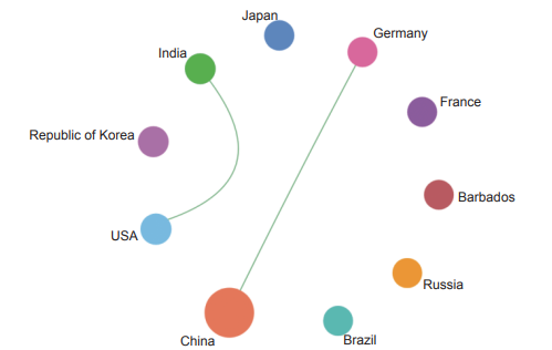
Figure 2.2.3 Collaboration network among major countries in the engineering development front of “control technology of unmanned systems based on brain–computer interface”
《Table 2.2.4》
Table 2.2.4 Institutions with the greatest output of core patents on “control technology of unmanned systems based on brain–computer interface”
| No. | Institution | Published patents | Percentage of published patents/% | Citations | Percentage of citations/% | Citations per patent |
| 1 | Beijing Institute of Technology | 8 | 1.72 | 51 | 3.79 | 6.38 |
| 2 | Academy of Military Medical Sciences, PLA Academy of Military Science | 8 | 1.72 | 25 | 1.86 | 3.12 |
| 3 | Tianjin University | 7 | 1.51 | 45 | 3.35 | 6.43 |
| 4 | Northwestern Polytechnical University | 7 | 1.51 | 19 | 1.41 | 2.71 |
| 5 | Shanghai University | 6 | 1.29 | 39 | 2.9 | 6.5 |
| 6 | Beihang University | 6 | 1.29 | 30 | 2.23 | 5 |
| 7 | Xi’an Jiaotong University | 6 | 1.29 | 27 | 2.01 | 4.5 |
| 8 | Southeast University | 5 | 1.08 | 38 | 2.83 | 7.6 |
| 9 | Zhejiang University | 5 | 1.08 | 20 | 1.49 | 4 |
| 10 | Beijing University of Posts and Telecommunications | 5 | 1.08 | 9 | 0.67 | 1.8 |
《Figure 2.2.4》

Figure 2.2.4 Roadmap of the engineering development front of “control technology of unmanned systems based on brain–computer interface”
systems to handle complex problems better and complete difficult tasks. From a practical standpoint, the current unmanned system technology based on brain–computer interfaces has undergone initial principle verification and entered the product research and development stage. It is expected that within 10 years, it will progress from principle prototypes to small-scale applications and eventually reach the multifield promotion and application stage. Brain–computer fusion is an inevitable trend in the development of unmanned systems based on brain–computer interfaces. The integration of “brain” and “machine” dual intelligence can bring many innovations and applications, and is expected to be used in traffic safety, aerospace, navigation, assistance for the elderly and disabled, medical assistance, rescue and disaster relief, industrial control, and other fields to produce more positive impacts.
2.2.3 Computing power network construction technology for diverse computing
With the rapid development of big data and AI technology, the demand for computing power and storage capacity in various industries is increasing. The main goal of computing power network construction technology for diverse computing is to build a computing power network that can meet the needs of heterogeneous computing to improve computational efficiency, reduce energy consumption, and solve the problems of insufficient computing and resources encountered by the traditional computing model when dealing with large-scale data and complex tasks. Computing power network construction technology for diverse computing can combine various computing resources to form a powerful computing power network that can better meet the computational needs of different application scenarios and realize efficient data computation and processing.
Computing power network construction technology for diverse computing has broad application prospects because it can integrate and optimize computing resources to achieve efficient computing capabilities. Governments worldwide are implementing several important plans for resource sharing between computing and data centers, and they have made some progress. The U.S. government has launched XSEDE, a federal program for sharing high performance computing and data resources to connect multiple high performance computing centers through a network to provide researchers and engineers with various computing and data resources. The European Union promoted the European Supercomputer Program (EuroHPC) to establish a Europe- wide supercomputing network to provide European research institutions and industry access to high performance computing resources through the PRACE supercomputer consortium. In addition, technology giants such as Google, Microsoft, and Amazon have launched their respective distributed cloud services or distributed computing engines to realize the cross-regional sharing and scheduling of large-scale resources. In the research field, the Lawrence Berkeley National Laboratory and Los Alamos National Laboratory in the USA have explored and experimented with large-scale scientific data sharing and the application of a unified runtime framework.
In China, research in this area is mainly conducted by scientific research institutions, universities, and telecommunication operators. In the context of the construction of channel computing resources from east to west and the Supercomputing Internet, the Computer Network Center of the Chinese Academy of Sciences has taken the lead in building a national high performance computing environment, effectively integrating high performance computing resources, and providing high performance computing services through a unified access portal. Emerging computing sharing platforms, such as the Integrated Computing Power Network of Shandong Province and China Smart computing power network led by Jinan Supercomputing and Peng Cheng Laboratory, are also developing, effectively promoting the interconnection and synergy of computing, data, software, and other resources in various provinces and municipalities.
Globally, several countries and regions are conducting research in this field. As shown in Tables 2.2.5 and 2.2.6, the USA is the country with the largest patent output in this field, accounting for 74.45%, indicating that the USA is a world leader in computing power network construction technology for diverse computing, with representative organizations such as U.S.-based EMC IP Holdings and International Business Machines Corporation. China has the second-largest patent output, accounting for 17.71%.
Computing power network construction technology for diverse computing usually requires close cooperation among multiple institutions and enterprises to achieve data sharing, technology synergy, and resource optimization. There is little cooperation among institutions and enterprises globally (Figure 2.2.5), and only the USA and India have cooperated, and the cooperation network among institutions has yet to be formed. Therefore, there is an urgent need to create cooperation network among countries and institutions to promote the development and application of this technology through joint scientific research, technology exchange, and project cooperation.
As shown in Figure 2.2.6, computing power network construction technology for diverse computing has the following key development directions in the next 5–10 years.
1) Computing power network architecture optimization: Perform computing power network architecture design and topology optimization based on Y.2501 computing power network framework. Better scheduling and management of computing resources will improve computing power and performance by establishing a more flexible and efficient basic communication network structure.
2) Heterogeneous resource convergence: In computing power networks, the convergence of different types of computing resources, such as central processing units, graphics processing units, and field-programmable gate arrays, will continue to evolve in-depth. Computing power networks will better use these heterogeneous resources to provide more efficient computing capabilities as computing resource innovations and performance improvements continue. For example, more powerful and efficient gas pedals, new server architectures, and processor designs have emerged to drive the development of computing power networks.
3) Cross-domain resource management and task collaboration: The goal of cross-domain resource management and task collaboration is to achieve the efficient use of computing resources and high performance in task execution. Computing power networks can make full use of computational resources from different domains through cross-domain resource management and task collaboration, improve resource utilization and performance, and collaborate in the execution of multiple tasks simultaneously to achieve more efficient computation and data processing. This is critical for promoting the development and application of diverse computing.
4) Computing operation and trading: computing trading is an important means of realizing spontaneous market regulation in the computing power network system and coordinating the benefits of each service subject. To realize reasonable billing, it is necessary to establish a spatiotemporal model of resource use through multidimensional and multigranular information collection of computing resource usage and load indicators to realize reasonable billing.
5) Convergence of AI and computing power network: The rapid development of AI technology will converge with computing power network to provide more powerful intelligence and learning capabilities for computing tasks. The computing power network will realize intelligent resource management and automated decision making by integrating AI algorithms and technologies,
《Table 2.2.5》
Table 2.2.5 Countries with the greatest output of core patents on “computing power network construction technology for diverse computing”
| No. | Country | Published patents | Percentage of published patents/% | Citations | Percentage of citations/% | Citations per patent |
| 1 | USA | 475 | 74.45 | 2 476 | 81.61 | 5.21 |
| 2 | China | 113 | 17.71 | 328 | 10.81 | 2.9 |
| 3 | Germany | 9 | 1.41 | 11 | 0.36 | 1.22 |
| 4 | Canada | 7 | 1.1 | 24 | 0.79 | 3.43 |
| 5 | Russia | 7 | 1.1 | 22 | 0.73 | 3.14 |
| 6 | UK | 7 | 1.1 | 8 | 0.26 | 1.14 |
| 7 | India | 5 | 0.78 | 5 | 0.16 | 1 |
| 8 | Netherlands | 4 | 0.63 | 0 | 0 | 0 |
| 9 | Japan | 2 | 0.31 | 4 | 0.13 | 2 |
| 10 | Ireland | 1 | 0.16 | 147 | 4.85 | 147 |
《Table 2.2.6》
Table 2.2.6 Institutions with the greatest output of core patents on “computing power network construction technology for diverse computing”
| No. | Institution | Published patents | Percentage of published patents/% | Citations | Percentage of citations/% | Citations per patent |
| 1 | EMC IP Holding Company | 67 | 10.5 | 168 | 5.54 | 2.51 |
| 2 | International Business Machines Corporation | 43 | 6.74 | 208 | 6.86 | 4.84 |
| 3 | Bank of America Corporation | 41 | 6.43 | 142 | 4.68 | 3.46 |
| 4 | Nuance Communications Incorporated | 25 | 3.92 | 110 | 3.63 | 4.4 |
| 5 | ReliaQuest Holdings Limited Liability Company | 18 | 2.82 | 26 | 0.86 | 1.44 |
| 6 | Microsoft Technology Licensing Limited Liability Company | 15 | 2.35 | 49 | 1.62 | 3.27 |
| 7 | Gamalon Incorporated | 11 | 1.72 | 49 | 1.62 | 4.45 |
| 8 | Intel Corporation | 10 | 1.57 | 12 | 0.4 | 1.2 |
| 9 | Beijing University of Posts and Telecommunications | 9 | 1.41 | 53 | 1.75 | 5.89 |
| 10 | Shandong Inspur Science and Technology Academy Company Limited | 9 | 1.41 | 1 | 0.03 | 0.11 |
《Figure 2.2.5》
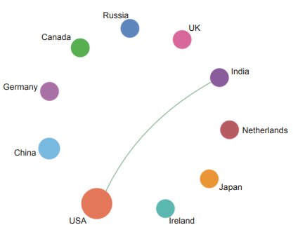
Figure 2.2.5 Collaboration network among major countries in the engineering development front of “computing power network construction technology for diverse computing”
《Figure 2.2.6》

Figure 2.2.6 Roadmap of the engineering development front of “computing power network construction technology for diverse computing”
such as deep learning, machine learning, and natural language processing, to provide more intelligent and adaptive computing capabilities.
6) Enhancement of security and privacy protection technologies: With the use of large-scale data and the distribution of computing resources, protecting data security and privacy will become an important concern in the development of computing power networks. Future computing power networks will enhance security techniques, such as data encryption, access control, and authentication, to ensure the security of computational tasks and data, and the protection of privacy.
In the future, computing power network construction technology for diverse computing will gradually become the core technology for data processing and analysis in various fields and will be widely used in cloud computing, big data analysis, AI, IoT, and other fields to promote the development and innovation of these fields. In addition, this technology has great development potential to provide more efficient and intelligent solutions for public safety, smart cities, medical health, industrial manufacturing, and other fields.
Participants of the Field Group
Review Members of the Expert Group
Leaders: PAN Yunhe, FEI Aiguo
Members (in alphabetical order):
Group 1: LIU Zejin, LUO Xiangang, LYU Yueguang, TAN Jiubin, ZHANG Guangjun
Group 2: DING Wenhua, DUAN Baoyan, HE You, WU Weiren, YU Shaohua
Group 3: CHAI Tianyou, CHEN Jie, FAN Bangkui, FEI Aiguo, LIAO Xiangke, LU Xicheng, PAN Yunhe, ZHAO Qinping
Subject Convenors (in alphabetical order)
CHEN Wenhua, CHENG Peng, LI Dongsheng, LIU Dong, LIU Jianguo, LIU Wei, LU Zhengang, PI Xiaodong,
XIN Bin, YANG Yi, ZHANG Jianhua
Library and Information Specialists
Literature: LI Hong, ZHAO Huifang, XIONG Jinsu, WANG Kaifei, CHEN Zhenying
Patent: YANG Weiqiang, LIANG Jianghai, LIU Shulei, HUO Ningkun, WU Ji, LIU Yi, YANG Zining
Report Writers (in alphabetical order)
For the engineering research fronts: CHEN Xiaoming, FANG Chongrong, GAO Fei, HAN Yahong, HAN Yu, HE Jianping,
JIN Shi, LI Ge, LIU Jianguo, LUO Junwei, WU Fei, XIE Tao, YU Haiyang, ZHANG Ying, ZHOU Ye, ZOU Canwen
For the engineering development fronts: CHEN Wenhua, FANG Bin, GAO Yang, HAO Aimin, HUANG Shanguo,
LIN Fenghan, LIN Jing, LIU Sha, LUO Huan, PI Xiaodong, TANG Zhuo, XIE Songyun
Working Group
Liaisons: GAO Xiang, ZHANG Jia, ZHANG Chunjie, DENG Huanghuang
Secretaries: ZHAI Ziyang, CHEN Qunfang, YANG Weiqiang, HU Xiaonv
Assistant: HAN Yushan


 京公网安备 11010502051620号


