
2021年 第7卷 第11期
《工程(英文)》 >> 2021年 第7卷 第11期 doi: 10.1016/j.eng.2020.08.019
基于超构表面等离激元透镜的高速并行近场直写纳米光刻系统
a State Key Laboratory of Advanced Design and Manufacturing for Vehicle Body, College of Mechanical and Vehicle Engineering, Hunan University, Changsha 410082, China
b State Key Laboratory of Tribology, Department of Mechanical Engineering, Tsinghua University, Beijing 100084, China
c College of Mechanical and Electronic Engineering, China University of Petroleum, Qingdao 266580, China
下一篇 上一篇
摘要
具有简单、高效、低成本和高灵活性等特点的纳米加工技术在纳米尺度基础研究和原型验证中不可或缺。研究已证明,采用表面等离激元的近场光刻技术(即等离激元光刻)是一种有前景的解决方案。基于高速旋转基底上高刚度被动纳米间隙控制的加工系统是其中一种高效率加工方案。但是,为了研发出新一代具有高分辨率且可靠高效的纳米加工技术,需要探索一种更小更稳定的纳米间隙和新型等离激元透镜及其并行加工方案。因此,本文设计了一套并行等离激元直写纳米光刻系统。该系统应用了新型等离子浮动磁头,当转速为8~18 m⋅s−1时,其最小飞行高度可实现15 nm并且具有高平行度。本文还研制了一种多级的基于超构表面的偏振不敏感等离激元透镜。与传统的等离激元透镜相比,该透镜耦合的功率更大,焦点的范围更集中。该原型系统实现了约26 nm最小线宽的纳米结构并行光刻。该系统有望应用于高自由级、低成本的纳米加工技术,如平面光学元件和纳米机电系统。
补充材料
图片
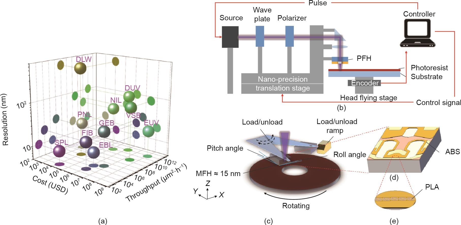
图1

图2

图3

图4
参考文献
[ 1 ] Gwyn CW, Stulen R, Sweeney D, Attwood D. Extreme ultraviolet lithography. J Vac Sci Technol B 1998;6(16):3142–9. 链接1
[ 2 ] Wu B, Kumar A. Extreme ultraviolet lithography: a review. J Vac Sci Technol B 2007;25(6):1743. 链接1
[ 3 ] Vieu C, Carcenac F, Pépin A, Chen Y, Mejias M, Lebib A, et al. Electron beam lithography: resolution limits and applications. Appl Surf Sci 2000;164(1– 4):111–7. 链接1
[ 4 ] Manfrinato VR, Zhang L, Su D, Duan H, Hobbs RG, Stach EA, et al. Resolution limits of electron-beam lithography toward the atomic scale. Nano Lett 2013;13(4):1555–8. 链接1
[ 5 ] Giannuzzi LA, Stevie FA. A review of focused ion beam milling techniques for TEM specimen preparation. Micron 1999;30(3):197–204. 链接1
[ 6 ] Melngailis J. Focused ion beam technology and applications. J Vac Sci Technol B 1987;5:469.
[ 7 ] Garcia R, Knoll AW, Riedo E. Advanced scanning probe lithography. Nat Nanotechnol 2014;9(8):577–87. 链接1
[ 8 ] Malinauskas M, Zˇukauskas A, Hasegawa S, Hayasaki Y, Mizeikis V, Buividas R, et al. Ultrafast laser processing of materials: from science to industry. Light Sci Appl 2016;5(8):e16133. 链接1
[ 9 ] Fang N, Lee H, Sun C, Zhang X. Sub-diffraction-limited optical imaging with a silver superlens. Science 2005;308(5721):534–7. 链接1
[10] Srituravanich W, Fang N, Sun C, Luo Q, Zhang X. Plasmonic nanolithography. Nano Lett 2004;4(6):1085–8. 链接1
[11] Luo X, Ishihara T. Surface plasmon resonant interference nanolithography technique. Appl Phys Lett 2004;84(23):4780–2. 链接1
[12] Wang L, Jin EX, Uppuluri SM, Xu X. Contact optical nanolithography using nanoscale C-shaped apertures. Opt Express 2006;14(21):9902–8. 链接1
[13] Liu ZW, Wei QH, Zhang X. Surface plasmon interference nanolithography. Nano Lett 2005;5(5):957–61. 链接1
[14] Uppuluri SMV, Kinzel EC, Li Y, Xu X. Parallel optical nanolithography using nanoscale bowtie aperture array. Opt Express 2010;18 (7):7369–75. 链接1
[15] Kim Y, Kim S, Jung H, Lee E, Hahn JW. Plasmonic nano lithography with a high scan speed contact probe. Opt Express 2009;17 (22):19476–85. 链接1
[16] Kim S, Jung H, Kim Y, Jang J, Hahn JW. Resolution limit in plasmonic lithography for practical applications beyond 2x-nm half pitch. Adv Mater 2012;24(44):OP337–44. 链接1
[17] Jung H, Kim S, Han D, Jang J, Oh S, Choi JH, et al. Plasmonic lithography for fabricating nanoimprint masters with multi-scale patterns. J Micromech Microeng 2015;25(5):055004. 链接1
[18] Lee WS, Kim T, Choi GJ, Lim G, Joe HE, Gang MG, et al. Experimental demonstration of line-width modulation in plasmonic lithography using a solid immersion lens-based active nano-gap control. Appl Phys Lett 2015;106 (5):051111. 链接1
[19] Park KS, Kim T, Lee WS, Joe HE, Min BK, Park YP, et al. Application of solid immersion lens-based near-field recording technology to high-speed plasmonic nanolithography. Jpn J Appl Phys 2012;51:8S2. 链接1
[20] Kim T, Lee WS, Joe HE, Lim G, Choi GJ, Gang MG, et al. High-speed plasmonic nanolithography with a solid immersion lens-based plasmonic optical head. Appl Phys Lett 2012;101(16):161109. 链接1
[21] Pan L, Park Y, Xiong Y, Ulin-Avila E, Wang Y, Zeng L, et al. Maskless plasmonic lithography at 22 nm resolution. Sci Rep 2011;1:175. 链接1
[22] Srituravanich W, Pan L, Wang Y, Sun C, Bogy DB, Zhang X. Flying plasmonic lens in the near field for high-speed nanolithography. Nat Nanotechnol 2008;3 (12):733–7. 链接1
[23] Ji J, Meng Y, Hu Y, Xu J, Li S, Yang G. High-speed near-field photolithography at 1685 nm linewidth with linearly polarized illumination. Opt Express 2017;25 (15):17571. 链接1
[24] Ji J, Hu Y, Meng Y, Zhang J, Xu J, Li S, et al. The steady flying of a plasmonic flying head over a photoresist-coated surface in a near-field photolithography system. Nanotechnology 2016;27(18):185303. 链接1
[25] Hu Y, Meng Y. Numerical modeling and analysis of plasmonic flying head for rotary near-field lithography technology. Friction 2018;6(4):443–56. 链接1
[26] Fukui S, Kaneko R. Analysis of ultra-thin gas film lubrication based on linearized Boltzmann equation: first report—derivation of a generalized lubrication equation including thermal creep flow. J Tribol 1988;2 (110):253–61. 链接1
[27] Palik ED. Handbook of optical constants of solids. Pittsburgh: Academic Press; 1998. 链接1
[28] Hu Y, Wu H, Meng Y, Wang Y, Bogy D. Head flying characteristics in heat assisted magnetic recording considering various nanoscale heat transfer models. J Appl Phys 2018;123(3):034303. 链接1
[29] Hu Y, Wu H, Meng Y, Bogy DB. Nanoscale thermal analysis for heat-assisted magnetic recording. J Appl Phys 2017;122(13):134303. 链接1
[30] Yu N, Genevet P, Kats MA, Aieta F, Tetienne JP, Capasso F, et al. Light propagation with phase discontinuities: generalized laws of reflection and refraction. Science 2011;334(6054):333–7. 链接1
[31] Khorasaninejad M, Chen WT, Devlin RC, Oh J, Zhu AY, Capasso F. Metalenses at visible wavelengths: diffraction-limited focusing and subwavelength resolution imaging. Science 2016;352(6290):1190–4. 链接1
[32] Hu Y, Luo X, Chen Y, Liu Q, Li X, Wang Y, et al. 3D-integrated metasurfaces for full-colour holography. Light Sci Appl 2019;8(1):86. 链接1
[33] Hu Y, Li L, Wang Y, Meng M, Jin L, Luo X, et al. Trichromatic and tripolarizationchannel holography with noninterleaved dielectric metasurface. Nano Lett 2020;20(2):994–1002. 链接1
[34] Lin J, Mueller JPB, Wang Q, Yuan G, Antoniou N, Yuan XC, et al. Polarizationcontrolled tunable directional coupling of surface plasmon polaritons. Science 2013;340(6130):331–4. 链接1
[35] Wang Y, Yao N, Zhang W, He J, Wang C, Wang Y, et al. Forming sub-32-nm high-aspect plasmonic spot via bowtie aperture combined with metal– insulator–metal scheme. Plasmonics 2015;10(6):1607–13. 链接1
[36] Kobayashi M, Horowitz R. Track seek control for hard disk dual-stage servo systems. IEEE Trans Magn 2001;2(37):949–54. 链接1
[37] Stipe BC, Strand TC, Poon CC, Balamane H, Boone TD, Katine JA, et al. Magnetic recording at 1.5 Pbm2 using an integrated plasmonic antenna. Nat Photonics 2010;7(4):484–8. 链接1
[38] Challener WA, Peng C, Itagi AV, Karns D, Peng W, Peng Y, et al. Gage, Heatassisted magnetic recording by a near-field transducer with efficient optical energy transfer. Nat Photonics 2009;24(5):190–1. 链接1
[39] Juang JY, Bogy DB, Bhatia CS. Design and dynamics of flying height control slider with piezoelectric nanoactuator in hard disk drives. J Tribol 2007;129 (1):161–70. 链接1
[40] Wu H, Bogy D. Use of an embedded contact sensor to study nanoscale heat transfer in heat assisted magnetic recording. Appl Phys Lett 2017;110 (3):033104. 链接1
[41] Ma Y, Ghafari A, Budaev BV, Bogy DB. Measurement and simulation of nanoscale gap heat transfer using a read/write head with a contact sensor. IEEE Trans Magn 2017;2(53):3300105. 链接1
[42] Liu L, Gao P, Liu K, Kong W, Zhao Z, Pu M, et al. Nanofocusing of circularly polarized Bessel-type plasmon polaritons with hyperbolic metamaterials. Mater Horiz 2017;4(2):290–6. 链接1


 京公网安备 11010502051620号


