

《1. Introduction》
1. Introduction
Surface acoustic wave (SAW) technology is currently extensively applied in physical and biochemical sensors [1], photonics [2] and quantum acoustics, communication, signal processing [3], and labs-on-a-chip [4]. The maximum working frequencies of many conventional SAW devices are up to a few gigahertz (GHz), which cannot meet the strong demands of ultra-high-frequency acoustic wave devices for future electronics and communications. It is essential for SAW devices to be operated at higher frequencies (> 3 GHz) for precision sensing [5], 5G communication, and quantum control of SAW-induced phonons [6], as well as integrated microwave-photonics signal processing [7].
A SAW device’s resonant frequency,  is linked to the acoustic wave velocity v; and the wavelength
  based on the formula
  Two methods are frequently used to increase the frequency of a SAW device. The most common approach is to reduce the value of
  by increasing the resolution of patterns using a nanoscale manufacturing technology [8]. Büyükköse et al. [9] reported that a SAW device based on a ZnO/SiO2/Si structure achieved a high frequency of 16.1 GHz using nanoimprint lithography. Using electron beam lithography (EBL), Mohammad et al. [10] achieved a high frequency of 14.2 GHz for a LiNbO3 SAW device with a wavelength of 200 nm. Our group recently reported a LiNbO3 SAW device with a 30 GHz frequency, which was made using an improved EBL process [11]. The second approach is to design and apply slow-on-fast structures by using a film with a low velocity on top of a substrate with a much higher acoustic velocity; examples include ZnO/SiC [12], AlN/SiC [13], ZnO/diamond [14], AlN/diamond [15], and AlN/Pt/diamond/Si [16]. Previously, our group reported that high frequencies of 33.7 GHz [17] and 17.7 GHz [18] were successfully obtained with SAW devices based on AlScN/diamond/Si and AlN/diamond/Si structures, using EBL technology.
However, several key issues remain to be solved: ① To reduce the value of , most researchers focus on pushing the dimension limits of interdigital transducers (IDTs) on a single-crystal substrate, such as LiNbO3, which possesses excellent surface smoothness and a high electromechanical coupling coefficient (K2 ). However, these single-crystal substrates often have low wave velocities and/or are incompatible with the complementary metal oxide semiconductor (CMOS) process. ② For slow-on-fast structure designs, the commonly used piezoelectric materials are ZnO or AlN, which have relatively low K2 values and thus severely affect the device’s performance. Recently, single-crystal film/SiC-based SAW devices on multilayered substrates of LiNbO3/SiC [19] or LiNbO3/SiO2/SiC [20] were utilized to make high-frequency SAW devices, especially SAW filters. However, previous studies have mainly focused on SAW devices with working frequencies lower than 5 GHz, without much focus on the potential of generating multiple acoustic modes for super-high-frequency applications.
To address these critical issues, we propose a hybrid strategy that integrates a nanomanufacturing process with a heterostructure design on a slow-on-fast substrate, which successfully breaks the frequency record for current SAW devices. Based on this novel idea, we develop heterostructures of LiNbO3/SiO2/SiC and apply EBL with a proximity effect correction (PEC) algorithm to optimize the dimensions of the SAW IDTs, thereby achieving an electrode finger width of 35 nm. The finite-element method (FEM) is applied to theoretically analyze and identify the higher order acoustic modes of the LiNbO3 film-based slow-on-fast SAW devices. We then successfully fabricate SAW devices with frequencies from 5 to about 44 GHz. Finally, we achieve a super-high mass sensitivity, thus demonstrating the superior sensing performance and potential application of the proposed ultra-high-frequency SAW platform.
《2. Experimental procedure》
2. Experimental procedure
Fig. 1(a) illustrates the overall structure of the proposed oneport ultra-high-frequency SAW resonator, which is manufactured on a LiNbO3/SiO2/SiC multilayered heterostructure. A 4 in (1 in = 2.54 cm) X cut 34° Y LiNbO3 single crystal was applied as the piezoelectric layer due to its relatively high K2 value and excellent surface smoothness, which are beneficial for device fabrication and performance. The detailed fabrication processes for the LiNbO3 single-crystal film on the slow-on-fast substrates are shown in Fig. S1 in Appendix A, and are based on a typical ion-cut process. SiC was applied as the carrier substrate because it exhibits large velocities for both shear waves (7100 m·s–1 ) and longitudinal waves (12 500 m·s–1 ) [21], low propagation loss, and high thermal conductivity. As is well-known, SiC is a third-generation semiconductor material that can be used to integrate microelectronic devices with SAW devices on a single chip [22]. In this multilayer design, SiO2 was applied as a temperature compensation layer. Fig. S2 in Appendix A presents a technological process diagram for the EBL and the lift-off for patterning the nanoscale IDTs. The optimized PEC algorithm for the EBL was reported in our previous work [11]. In the present work, SAW devices with wavelengths from 160 to 800 nm were prepared. The IDTs had a pair number of 50, and the aperture (L) was 20. The reflectors were separated from the IDTs by a distance of 0.25. Detailed geometrical information for the SAW devices is summarized in Table S1 in Appendix A.
The fabricated structures of the IDTs and the cross-section morphology of the LiNbO3/SiO2/SiC multilayer were checked using a scanning electron microscope (SEM) (Carl-Zeiss Sigma HD, Germany). An X-ray diffractometer (XRD) (D8 ADVANCE, Germany) was used to characterize the crystalline structure of the films. The surface topography of the LiNbO3 film/SiO2/SiC multilayer was investigated using an atomic force microscope (AFM) (SPI-3800N, Seiko Co., Japan). Device performance was characterized using a Rohde & Schwarz vector network analyzer (with a maximum frequency of up to 67 GHz), together with an MPI Corporation 200 mm automated engineering probe system (MPI TS2000-SE) and ground (G)–signal (S)–ground (G) probes. Before making scatter-parameter (S) measurements of the fabricated SAW devices, we used calibration chips for the different cases of an open circuit, a short circuit, and load calibration, in order to minimize the parasitic parameters generated by the radio frequency cable and probe test equipment.
The sensing mechanism for mass detection was based on the loading effect of Au IDT electrodes, as reported in our previous work [23]. Different Au IDT thicknesses of 20 nm (defined as zero mass loading) and 25 nm (with an estimated mass loading of 0.0966 μg∙mm–2 ) were employed as different mass loadings on the SAW device; changes in the frequency signals were then obtained. In this study, Au was selected as the material for the IDT electrodes, as it exhibits better electrical conductivity than aluminum and, during the lift-off process, shows less defect formation and failure of the IDTs.
The temperature effects on the responses of the SAW devices were studied using a probe system and a network analyzer with a LabVIEW program. The MPI probe system has an integrated thermal chuck (20–300 °C) with a touchscreen display placed conveniently in front of the operator for fast operation and immediate feedback. The SAW samples were placed on the loading chuck of the probe system during the test, and the G–S–G probe was used to connect the SAW IDTs to the network analyzer. We used the touchscreen display to adjust the temperature and heated the loading chuck inside the equipment to adjust the temperature to the set point. We then recorded the changes in the frequency signals.
《3. Results and discussion》
3. Results and discussion
Fig. 1(b) presents an SEM image of a SAW device based on a LiNbO3/SiO2/SiC heterostructure. The image shows that the single-crystal LiNbO3 films are seamlessly bonded onto the SiO2/ SiC substrate. The thicknesses of the LiNbO3 film and the SiO2 film on the SiC carrier substrate are approximately 220 and 140 nm, respectively. Fig. 1(c) provides an AFM image showing the surface morphology of the SAW device. The roughness value of the LiNbO3 film is about 0.615 nm (a root mean square (RMS) value), which is much smaller than those of the AlN or ZnO film-based slow-on-fast substrates reported in the literature [12–16]. A smooth surface is vital to push the frequency limit by reducing the IDT finger width via improved patterning resolution using nanomanufacturing technology. Fig. 1(d) shows the XRD spectra of the LiNbO3 film on the SiC substrate. There is only one peak at a two theta angle of about 34°, demonstrating that the LiNbO3 film is highly oriented (110). Fig. 1(e) provides an optical image of the SAW device. Fig. 1(f) presents the complete IDTs, demonstrating that our optimized manufacturing method using improved EBL can successfully achieve nanoscale patterns on IDTs. Figs. 1(g)–(l) presents a series of SEM images of SAW IDTs with wavelengths of 160, 200, 320, 400, 600, and 800 nm. It is clear that an ultra-high-resolution IDT finger with a 160 nm wavelength and a width of approximately 35 nm (Fig. S3 in Appendix A) has been realized. By means of a thorough literature survey, we confirmed that this value is the smallest wavelength among all reported slow-on-fast layer structure SAW devices to date.
《Fig. 1》
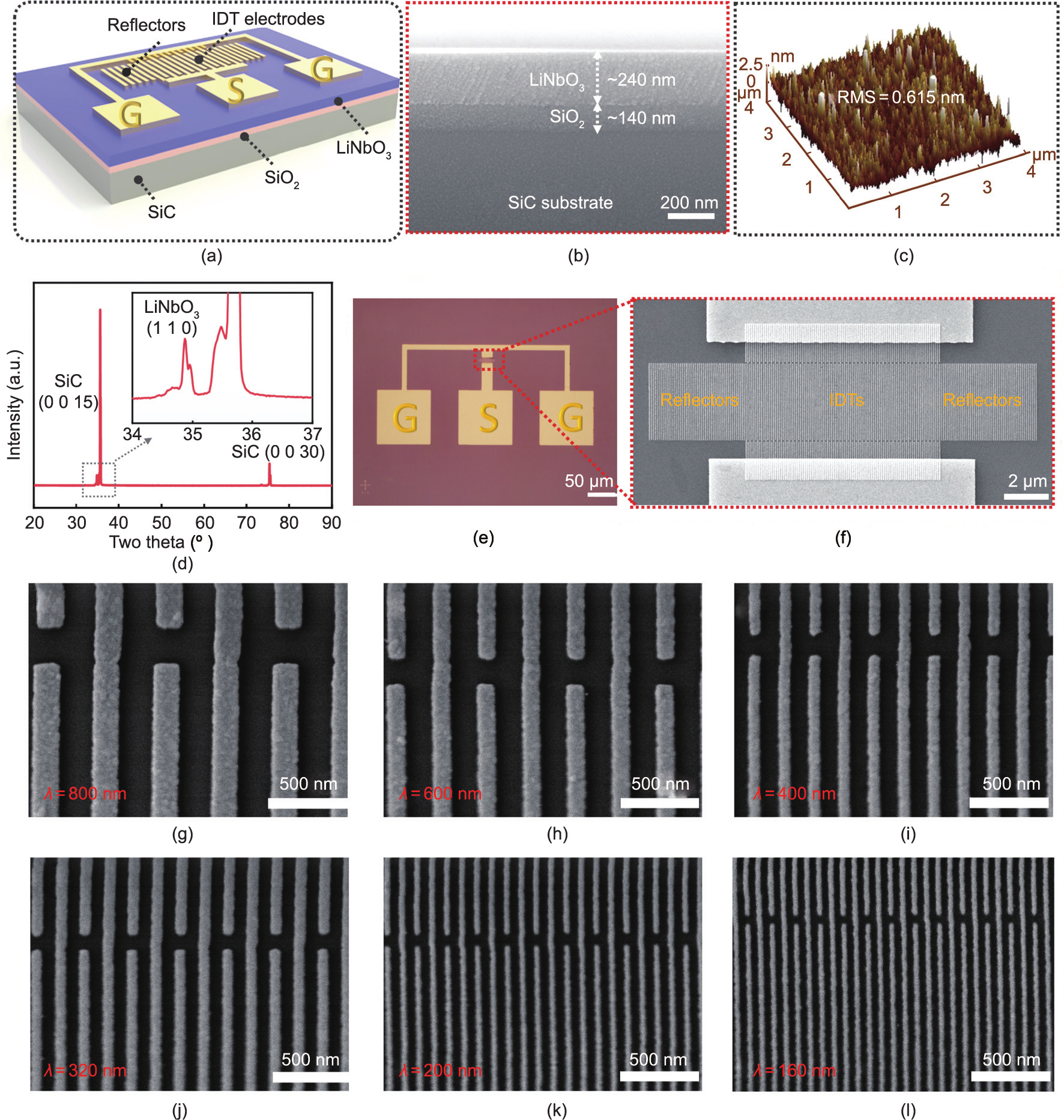
Fig. 1. (a) Schematic illustration of the proposed one-port SAW device using a LiNbO3/SiO2/SiC heterostructure; (b) cross-section morphology of the LiNbO3/SiO2/SiC heterostructure; (c) atomic force microscope (AFM) micrograph of the LiNbO3/SiO2/SiC substrate; (d) X-ray diffractometer (XRD) pattern of the LiNbO3/SiO2/SiC substrate; (e) optical image of the fabricated SAW with a of 160 nm; (f–l) scanning electron microscope (SEM) images of IDTs with the number of both the IDT pairs and the reflectors being set at 50 and different of 800, 600, 400, 320, 200, and 160 nm. RMS: root mean square; a.u.: arbitrary unit.
The admittance curves (Y11) of the various fabricated devices are shown in Fig. 2, and the reflectance signals (S11) of the fabricated SAW devices are presented in Fig. S4 in Appendix A. Multiple acoustic modes can be observed for all the SAW samples. The range of resonant frequency increases from 4–15 to 10–42 GHz as the wavelength decreases from 800 to 160 nm. The signal amplitude decreases slightly with a decrease in wavelength, which can be attributed to the increased impedance of the devices with much finer IDT patterns. In addition, it is difficult to obtain uniform IDT fingers for smaller wavelength devices, which results in relatively weak signals. Nevertheless, a high frequency value of about 41.5 GHz was recorded for the fabricated device with a wavelength of 160 nm. Furthermore, we fabricated four SAW samples with the same of 160 nm to verify that the high frequency we obtained was not due to parasitic responses or noises. All these devices displayed similar results, as shown in Fig. S5 in Appendix A, indicating that the obtained frequency signal was induced by SAWs.
To verify the modes of these multiple peaks, we conducted a numerical analysis using the FEM method (with COMSOL software) and obtained the admittance values of SAW devices with different wavelengths. Fig. 2 presents the obtained analysis results, which indicate that the simulated frequency signals of the samples with various wavelengths are in good agreement with the experimental results. A detailed theoretical analysis and the experimentally obtained results of the SAW devices’ frequencies are provided in Appendix A.
《Fig. 2》
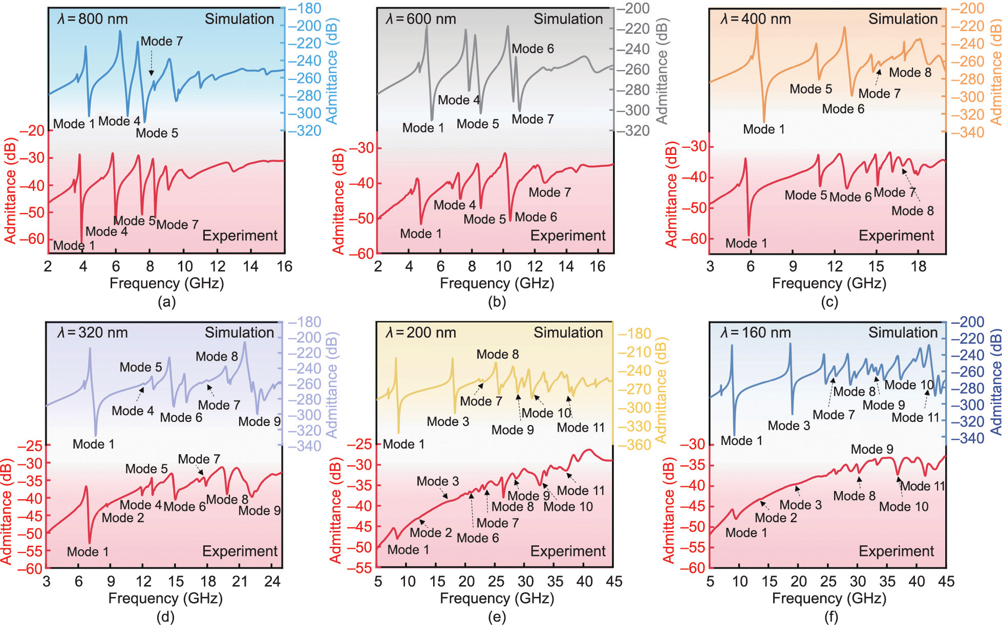
Fig. 2. Admittance and resonant frequency performance spectra for SAW samples with different of 800, 600, 400, 320, 200, and 160 nm, where the red line is the admittance of the experimental SAW devices and the upper line is the admittance characteristic from the FEM simulation. Mode 1: shear–horizontal (SH) wave; Mode 2: Rayleigh wave; Mode 3: longitudinal SAW coupled with a harmonic metal thickness; Mode 4: a longitudinal SAW; Mode 5: a high-order SH mode; Modes 6–11: high-order SAWs that propagate near the SiC substrate.
To further confirm the multiple modes of these SAW devices, an eigenfrequency analysis was conducted to investigate the particle vibration patterns. Fig. 3(a) presents the particle vibration pattern of each mode for the ultra-high-frequency SAW devices. The figure clearly shows that Mode 1 corresponds to the shear–horizontal (SH) wave mode, and its particle displacements and wave vibrations mainly exist along the direction of the horizontal aperture [20], as shown in Fig. S6(a) in Appendix A. Mode 2 is a standard Rayleigh wave [11], Mode 3 is a longitudinal SAW coupled with a harmonic metal thickness mode [24], Mode 4 is a longitudinal SAW [25], and Mode 5 is a high-order SH mode. All other modes are high-order SAWs that propagate near the SiC substrate [26]. It is notable that, with a decrease in SAW wavelength, more acoustic modes are excited and detected, as illustrated in Fig. 3(a). This is mainly due to the layered structure of the SAW devices, the submicron thickness of the piezoelectric film, and the enhanced interference effect that occurs with a decrease in SAW wavelength. For example, as shown in Fig. 3(a), the Rayleigh mode (Mode 2) is observed only if the wavelength is smaller than 320 nm. In addition, Modes 10 and 11 are detected only when the wavelength is below 200 nm. These findings clearly show that a greater number of higher order SAW modes are generated when the wavelength is smaller than the thickness of the layer [27].
《Fig. 3》
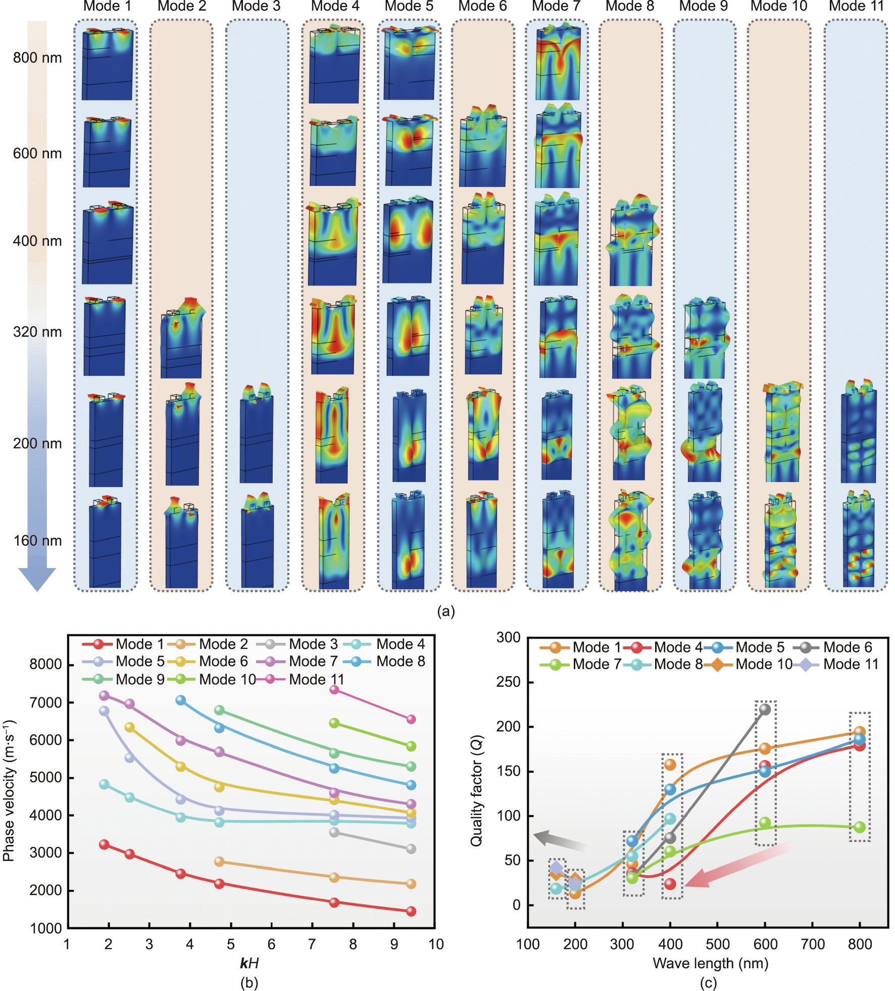
Fig. 3. (a) Particle displacements of multiple modes for the SAW with ranging from 800 to 160 nm; (b) phase velocity vs normalized film thickness on the LiNbO3/SiO2/SiC structure (kH) SAW, where H is the thickness of LiNbO3 and k is the wave vector; (c) Q values vs wavelengths for the SAW with ranging from 800 to 160 nm.
The phase velocities of different wave modes as a function of the normalized thickness kH ( where H is the thickness of LiNbO3 and k is the wave vector) are summarized in Fig. 3(b). It is clear that, with an increase of kH, the phase velocities of all these modes decrease, mainly because more acoustic energy is confined inside the LiNbO3 layer, whose acoustic velocity is much smaller than that of the substrate.
The Bode-quality factors (Q) [28] of the SAW resonators with varied wavelengths can be calculated as follows:

where (S11)group_delay is the group delay of the S11 parameters and ω is the angular frequency. The measured Bode-Q curves of devices with different wavelengths are shown in Fig. S7 in Appendix A. Table S2 in Appendix A and Fig. 3(c) summarize the calculated Q values for SAW resonators with different wavelengths. With an increase in SAW wavelength, the Q value of each mode increases, as shown in Fig. 3(c), except for Modes 10 and 11. The decreased Q values for these cases with smaller wavelengths can be explained by the greater impedance values of the SAW devices with extremely narrow IDT fingers, the higher acoustic loss, and the non-uniformity of IDT widths produced by nanoscale fabrication. The higher order Modes 10 and 11 are generated only for the IDT wavelengths of 200 and 160 nm. This is because the interference effect generated by the wave reflection from the SiC substrate is significantly enhanced when is smaller than the thickness of the LiNbO3 [27]; thus, a smaller wavelength is beneficial for the generation of higher modes for the ultra-high-frequency SAWs [18]. The Q values of both Mode 10 and Mode 11 increase when the SAW devices’ wavelength is decreased (from 200 to 160 nm) because of the increased interference effect of reflected acoustic waves from the substrate.
The effective coupling coefficient ( ) can be calculated as follows:

where  and
and  are the anti-resonant and resonant frequencies, respectively, of the admittance curves for the SAW resonators. Table S3 in Appendix A summarizes the obtained values of all the SAW devices. The results show that Mode 1 (SH wave) has a higher value, compared with the higher modes, which is consistent with the theoretical simulations (Table S3 in Appendix A). A high value of 15.7% is obtained for the device with a frequency of approximately 10 GHz (SH wave) and a wavelength of 160 nm. In contrast, for the device with a frequency of 41.5 GHz (Mode 11) at the same wavelength of 160 nm, the value becomes 7.3%. A detailed analysis of the SH mode, which has relatively good performance and a large , is summarized in Fig. S6 in Appendix A.
To demonstrate the application of these ultra-high-frequency SAW devices, we conducted mass detection tests by mass loading onto the IDTs of the SAW devices [23]. Two different IDT thicknesses—that is, 20 nm (which was assigned as the original state without any mass loading) and 25 nm (corresponding to a mass loading of 0.0966 μg·mm–2 on the IDTs)—were fabricated for the SAW devices. Figs. 4(a) and (b) and Fig. S8 in Appendix A show the mass sensing results using the fabricated SAW samples with wavelengths of 320, 200, and 160 nm. When mass was added onto the IDTs, the frequency value of the SAW device decreased for all these wavelengths. The sensitivity of the SAW device can be calculated using the changes in frequency divided by the mass changes per sensing area [29], using the following formula:

where  is the shift in the frequency,
  is the mass loading, S is the mass sensitivity, and A is the sensitive area. Table S4 in Appendix A summarizes the obtained mass sensitivity values for all the modes for samples with various wavelengths. The results show that the devices with smaller wavelengths have much greater mass sensitivities, due to their higher working frequencies. As shown in Fig. 4(c), as the device’s wavelength is decreased from 320 to 160 nm, its shift in frequency increases from 648.9 to 1527.9 MHz. These findings indicate the dramatically increased mass sensitivity values for the SH modes—namely, 6717.1, 10183.9, and 15817.5 MHz·mm2 ·μg–1 for the respective wavelengths of 320, 200, and 160 nm.
For a fixed wavelength, different modes have different sensitivity values. As shown in Fig. 4(c), the frequency shifts for the SH wave mode and the Rayleigh wave mode are quite different under the same mass loading for all the wavelengths. Although the SH wave mode has a lower frequency, its sensitivity is much higher than that of the Rayleigh wave. This is because the SH wave’s velocity is more sensitive to the mass loading on the electrode, especially for heavy metal films [30].
《Fig. 4》
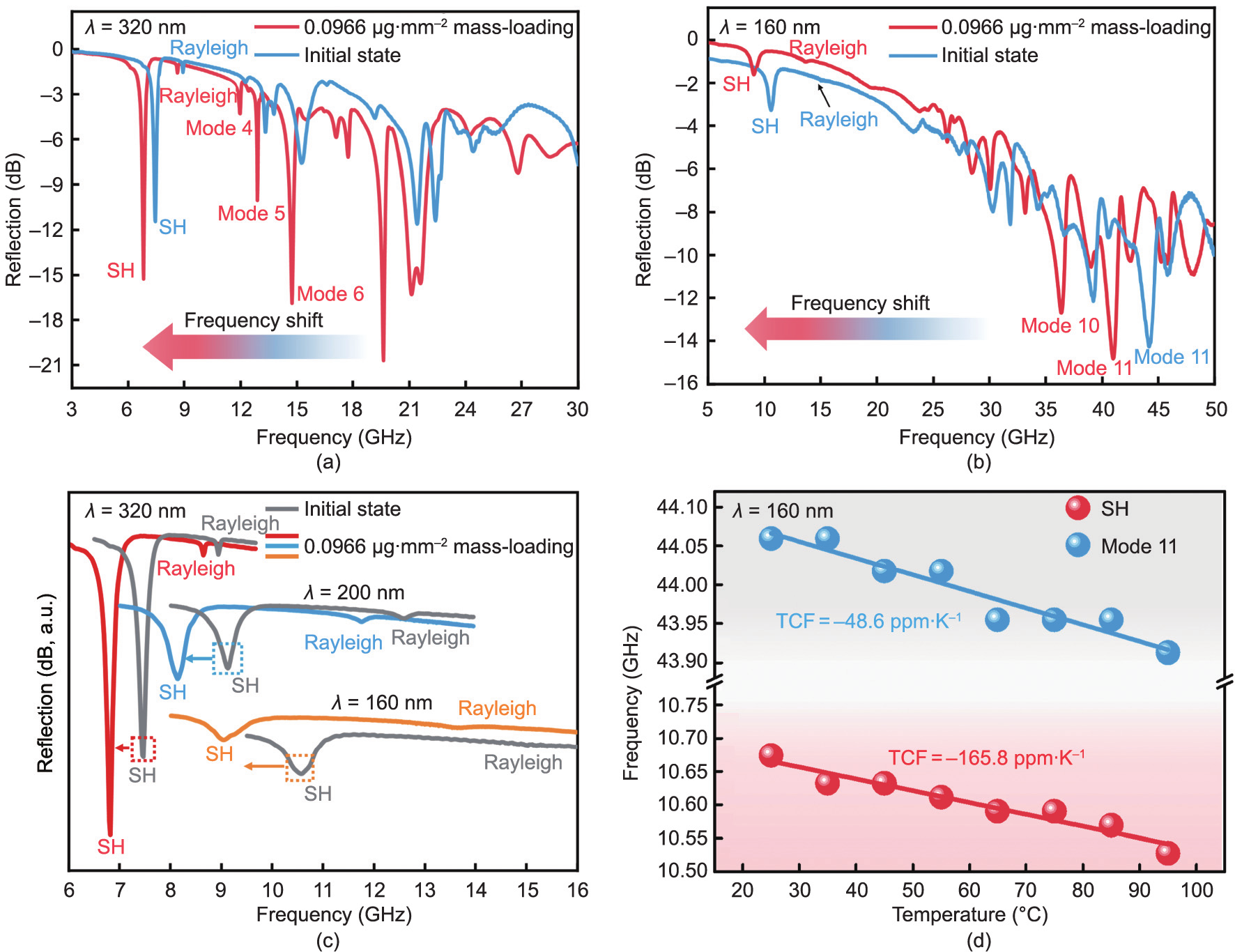
Fig. 4. Frequency shift of the fabricated SAW device with a of (a) 320 nm and (b) 160 nm and a mass loading of 0.0966 μg·mm–2 on IDTs; (c) frequency responses of the SH and Rayleigh modes for a from 320 to 160 nm and a mass loading of 0.0966 μg·mm–2 on IDTs; (d) resonant frequency shift of a device with a of 160 nm versus temperature for the SH and Mode 11. TCF: temperature coefficient of frequency.
We calculated all the mass sensitivity values for the SAW devices (Table S4 in Appendix A). The results show that Mode 11 possesses much higher sensitivity values than the other modes. The highest mass sensitivity for all the SAW devices is about 33151.9 MHz·mm2 ·μg–1 for Mode 11 with a frequency of 44.2 GHz. Based on an extensive literature search, we can confirm that this frequency value is the highest reported frequency value for a SAW device to date. Compared with the mass sensitivity results of a conventional quartz crystal microbalance (QCM) and a standard SAW device with a frequency of 978 MHz, as reported in the literature and listed in Table 1 [31–36], the corresponding value of the SAW device obtained in this study is about 1011 times higher than the former and about 4000 times higher than the latter.
《Table 1》
Table 1 Comparisons of mass sensitivity for SAW and QCM devices.

The temperature characteristics of the SAW devices is another important parameter for application. The temperature coefficient of frequency (TCF) of a SAW device can be calculated as follows:
where  is the SAW device’s resonant frequency at room temperature and
  is the temperature shift. For the LiNbO3/SiO2/SiC-based SAWs with wavelengths of 160 and 200 nm, the obtained TCF values are summarized in Fig. 4(d) and Fig. S9 in Appendix A. As the SH wave mode has the best performance and Mode 11 has highest sensitivity values, we only show the TCF results of these two modes. The results clearly reveal a linear trend in the frequency shift as a function of temperature, as shown in Fig. 4(d). The TCF values are –165.8 and –229.0 ppm·K–1 for the SH modes, and about –48.6 and –55.2 ppm·K–1 for Mode 11; this indicates that Mode 11 is slightly less sensitive than the SH modes to temperature changes. In order to verify the TCF values that were measured experimentally, we calculated the theoretical temperature effects of the SH mode for SAW devices with a wavelength of 160 nm. The obtained theoretical TCF value is approximately –154.4 ppm·K–1 (Fig. S10 in Appendix A), which is close to the experimentally obtained result of –165.8 ppm·K–1 .
《4. Conclusions》
4. Conclusions
In this paper, we proposed a hybrid strategy to integrate a nanomanufacturing process with a heterostructural (slow-onfast) design of LiNbO3/SiO2/SiC to increase the frequency of a SAW device. We demonstrated that SAW devices with frequencies of 5–44 GHz could be obtained, with large electromechanical coupling coefficients. The proposed LiNbO3/SiO2/SiC heterostructures exhibit multiple modes; we performed a theoretical analysis and identified these higher order guided wave modes. Furthermore, we systematically investigated the mass sensitivity characteristics of these modes and found that the SH mode has the best SAW resonance characteristics and is very sensitive to mass loading, indicating that it holds great potential for high-frequency sensing applications. Mode 11 possesses a much higher sensitivity value than the other modes and exhibits a relatively low TCF value. An ultra-high mass sensitivity of about 33151.9 MHz·mm2 ·μg–1 was achieved using this mode. This value is approximately 1011 times higher than a conventional QCM device and about 4000 times higher than a standard SAW device with a frequency of 978 MHz.
《Acknowledgments》
Acknowledgments
This study was supported by the National Science Foundation of China (NSFC) (52075162), the Program of New and High-Tech Industry of Hunan Province (2020GK2015 and 2021GK4014), the Excellent Youth Fund of Hunan Province (2021JJ20018), the Key Program of Guangdong (2020B0101040002), the Joint Fund of the Ministry of Education (Young Talents), the Natural Science Foundation of Changsha (kq2007026), the Tianjin Enterprise Science and Technology Commissioner Project (19JCTPJC56200), and the Engineering Physics and Science Research Council of the United Kingdom (EPSRC EP/P018998/1).
《Compliance with ethics guidelines》
Compliance with ethics guidelines
Jian Zhou, Dinghong Zhang, Yanghui Liu, Fengling Zhuo, Lirong Qian, Honglang Li, Yong-Qing Fu, and Huigao Duan declare that they have no conflict of interest or financial conflicts to disclose.
《Appendix A. Supplementary data》
Appendix A. Supplementary data
Supplementary data to this article can be found online at https://doi.org/10.1016/j.eng.2022.05.003.


 京公网安备 11010502051620号


