
《1. Introduction》
1. Introduction
Photoelectrochemical (PEC) water splitting is an attractive technology for converting solar energy into storable hydrogen fuel, due to its ease of usage, storage, and transportation [1,2]. In the water splitting process, the four-electrons-involved oxygen evolution reaction (OER) occurring at the photoanode has resulted in sluggish kinetics. Compared to the hydrogen evolution reaction (HER) at the photocathode, the four electrons transfer process is demanded higher energy and then believed to act as the ratelimiting step for water splitting. Thus, it is highly desirable to develop stable and efficient photoanodes for PEC water oxidation, which remains a pivotal challenge in achieving practical solar water splitting [3,4].
Among various semiconductors, n-type silicon (n-Si) is considered to be a potential photoanode material for solar water splitting, due to its narrow band gap (1.12 eV, 1 eV = 1.60219 × 10⁻¹⁹ J) that matches the solar spectrum well, which endows the n-Si photoanode with a high theoretical photocurrent density (~43.7 mA∙cm–2) for photoanodic water oxidation [4,5]. Unfortunately, n-Si is very easily corroded or passivated in aqueous electrolytes, with inherent Fermi-level pinning at the surface states, which results in sluggish OER kinetics at the n-Si/electrolyte interface and thus leads to an undesirably large overpotential for water oxidation. Therefore, to achieve a reasonable photoconversion efficiency for solar water splitting, surface-deposited protective layers are indispensable to protect n-Si-based photoanodes from corrosion and passivation [6–22]. These protective layers are expected to simultaneously boost charge separation at the formed protective layer/Si junctional interface and serve as an effective electrocatalyst to accelerate the water oxidation kinetics at the photoanode/electrolyte interface [10–16]. As previously reported, iridium (Ir) and ruthenium (Ru) oxides, as benchmark water oxidation electrocatalysts, significantly reduce the overpotential required for the OER [23,24]. However, they are easily translated into IrO3 and RuO4 at a high anodic bias (~1.3 V vs reversible hydrogen electrode (RHE)) and then dissolve in the solution, making them unsuitable as protective layers [6,25]. Moreover, their high cost and scarcity limits their large-scale application in water splitting.
To replace noble metal catalysts, chemically stable and earthabundant transition-metal oxides (e.g., TiO2, NiOx, Fe2O3, etc.) have been coated onto bare n-Si photoanodes as protective layers for sustainable PEC water oxidation [8,9,11,16]. Furthermore, polymetallic oxides with highly active species exhibit excellent OER performance [17,18]. For example, an iron (Fe)-treated NiO/ p+n-Si photoanode with highly active species exhibited observably improved PEC performance, as compared with NiO/p+n-Si; in particular, the incorporation of Fe enhanced the stability of the NiO/p+n-Si photoanode during the PEC reaction [17]. Nevertheless, relative to these metal oxides with an intrinsic band gap and relatively high electrical resistance, metallic alloys with desirable electrical conductivity could be beneficial to the charge carrier transfer processes, and could thus contribute to a superior PEC performance for water splitting over a surface-coated n-Si photoanode [19–22]. For example, an n-Si photoanode covered with a 1 nm NiFe bimetallic layer exhibited a low onset potential at 1.06 V versus RHE and a high photocurrent density of 25.4 mA∙cm–2 at 1.23 V versus RHE in 1 mol∙L–1 NaOH under air mass 1.5 global (AM 1.5G) simulated solar illumination [21]. Unfortunately, the stability was unsatisfactory, with a saturated photocurrent density decreased greatly from about 30 to about 20 mA∙cm–2 in 24 h in 1 mol∙L–1 NaOH, which was related to the surface corrosion of the thin metallic NiFe layer. Although the n-Si/NiFe photoanode was stabilized by increasing the thickness of the NiFe layer to 2 nm, the photocurrent density at 1.23 V versus RHE was much lowered, reaching only 6.8 mA∙cm–2, due to the increased electrical resistance of the thickened NiFe layer. Thus, it is still highly challenging to obtain a metallic alloy overlayer that can efficiently catalyze OER and meanwhile stabilize the n-Si photoanode from surface corrosion and passivation in an alkaline solution. This challenge inspires us to further regulate the chemical compositions and the morphological/electronic structures of the metallic overlayer in order to synergistically boost the stability and activity of n-Si-based photoanodes for PEC water oxidation.
In this work, a trimetallic NiFeCo protective layer was coated onto a p+n-Si wafer by underpotential deposition (UPD). The obtained NiFeCo/p+n-Si photoanode exhibited highly efficient and stable PEC performance for the OER under simulated solar light. With UPD times and Ni:Fe:Co feeding molar ratios well optimized, the Ni0.9Fe0.05Co0.05/p+n-Si photoanode reached a remarkable photocurrent density (Jph) of about 33.1 mA∙cm–2 at 1.23 V versus RHE, with a low onset potential (Von is defined as the voltage corresponding to be required for driving water oxidation at a photocurrent density of 1.0 mA∙cm–2) of 0.938 V versus RHE.
Detailed characterizations and theoretical calculations demonstrated that the regulated band structure at the NiFeCo/p+n-Si interface and the modulated electronic structure of the NiFeCo protective layer synergistically contributed to the excellent PEC performance:
(1) The thin metallic NiFeCo layer, which has superior electrical conductivity, facilitates the charge carrier transfer processes; then, the in situ formed metallic (hydr)oxide layer acts as an excellent OER catalyst and efficiently catalyzes the water oxidation reaction.
(2) The introduction of Fe regulates the interfacial band structure, resulting in a large band bending and then promoting charge separation at the NiFeCo/p+n-Si interface.
(3) The incorporation of cobalt (Co) modulates the electronic structure of the trimetallic layer, producing abundant active sites and then accelerating the OER kinetics.
Furthermore, a low-cost photovoltaic (PV)/PEC device was fabricated for unassisted solar-driven water splitting, by coupling the NiFeCo/p+n-Si photoanode (0.51 cm2 ) with an inexpensive silicon (Si) solar cell (1 cm2 ). During 20 h continuous and bias-free operation, a high operating photocurrent of 14.8 mA and a stable solar-to-hydrogen (STH) conversion efficiency of 12.0% were achieved under simulated solar illumination.
《2. Results and discussion》
2. Results and discussion
A trimetallic NiFeCo protective layer was coated onto a p+n-Si wafer immersed in a NiSO4/FeSO4/CoSO4 mixture solution via UPD (Fig. S1 in Appendix A). The UPD times (750, 1000, and 1250 s) and Ni:Fe:Co feeding molar ratios (varying from 2:4:4 to 9:0.5:0.5) in the precursor solutions were tuned to adjust the chemical compositions of the deposited NiFeCo layers in order to optimize the PEC activity and stability of the obtained NiFeCo/ p+n-Si photoanodes. As shown in Fig. S2(a) (Appendix A), a NiFeCo layer deposited in 750 s could hardly prevent the n-Si surface from corrosion and passivation, as the obtained NiFeCo/p+n-Si (750 s) photoanode exhibited photocurrent densities greatly degenerated during continuous cyclic voltammetry (CV) measurements. Fortunately, by prolonging the UPD time to 1000 s, the deposited NiFeCo layer effectively stabilized the p+n-Si photoanode for efficient PEC water oxidation (Fig. S2(b) in Appendix A), with no decay in photocurrent density being observed during 3600 s reaction. When the UPD time was further prolonged to 1250 s, the obtained photoanode also stably operated in an alkaline electrolyte, but it exhibited a much lower PEC activity for water oxidation, with the Von anodically shifted and the Jph obviously decreased (Fig. S2(a)). These results indicate that 1000 s of UPD for NiFeCo deposition is enough to stabilize the p+n-Si photoanode.
Subsequently, the Ni:Fe:Co molar ratios in the precursor solutions were tuned to modulate the chemical composition and electronic structures of the deposited NiFeCo protective layer in order to efficiently catalyze PEC water oxidation. As shown in Fig. S3 in Appendix A, when the Ni:Fe:Co molar ratio was tuned to 9:0.5:0.5, the obtained Ni0.9Fe0.05Co0.05/p+n-Si photoanode presented excellent PEC performance, with a lowest Von of 0.938 V versus RHE and a highest Jph of about (33.10 ± 0.20) mA∙cm–2 at 1.23 V versus RHE. In the following sections, all analyses and discussions refer to the Ni0.9Fe0.05Co0.05/p+n-Si photoanode, unless specifically noted.
It is generally accepted that the electronic and morphological structures of the protective layer determine the stability and activity of n-Si-based photoanodes. Herein, X-ray photoelectron spectroscopy (XPS) was used to explore the surface chemical and electronic structures of the trimetallic-layer-coated p+n-Si photoanode (Ni0.9Fe0.05Co0.05/p+n-Si), compared with photoanodes coated with monometallic and bimetallic layers (e.g., Ni/p+n-Si and Ni0.9Fe0.1/p+n-Si) as references. As shown in Fig. 1(a), for Ni/p+n-Si, the Ni 2p3/2 peak can be deconvoluted into three peaks located at 852.4, 855.3, and 856.5 eV, which can be assigned to Ni0 , Ni2+, and Ni3+, respectively, indicating that nickel (Ni) (hydr)oxides are formed in situ at the surface of the deposited metallic Ni layer during UPD [26–28]. With the introduction of Fe, the Ni0 XPS peak almost disappears for Ni0.9Fe0.1/p+n-Si, implying that the metallic Ni0 species is converted to oxidized Ni2+/Ni3+ species at the surface. In a further comparison, for Ni0.9Fe0.05Co0.05/p+n-Si with Fe and Co simultaneously incorporated, the Ni2+ XPS peak intensity is greatly reduced, with the Ni3+ contents increasing from 44.84% for Ni/p+n-Si to 47.95% for Ni0.9Fe0.1/p+n-Si and then to 66.22% for Ni0.9Fe0.05Co0.05/p+n-Si (orange region, Fig. 1(a)). This observed increase in the Ni3+:Ni2+ molar ratios depending on Fe and/or Co incorporation demonstrates that the introduction of the Fe and Co elements (especially Co) creates abundant Ni3+ active sites at the surface of the deposited Ni0.9Fe0.05Co0.05 layer [29–31]. Fig. 1(b) shows the O 1s XPS spectra, which can be deconvoluted into four peaks associated with typical metal–oxygen bonding (M–O), oxygen vacancies (Ov), oxygen in hydroxyl groups (M–OH), and absorbed water (H2O), respectively [27,32–35]. It is clear that the M–O peak shifts to a higher binding energy for Ni0.9Fe0.05Co0.05/p+n-Si (529.8 eV), as compared with that for Ni/p+n-Si (529.3 eV) and Ni0.9Fe0.1/p+n-Si (529.6 eV), implying that the incorporation of Fe and/or Co triggers a charge redistribution of the Ni–O bond. Moreover, with the incorporation of Fe and Co, the percentage of the Ov peak (~530.7 eV) increases from 10.04% for Ni/p+n-Si to 13.50% for Ni0.9Fe0.1/p+n-Si, and then to 32.31% for Ni0.9Fe0.05Co0.05/p+n-Si (pink region, Fig. 1(b)), accounting for the increased Ov concentration with lowered oxygen coordination at the surface [36,37]. All these XPS analysis results demonstrate that the incorporation of Fe and Co into the metallic Ni layer modulates the electronic structure and then produces more Ni3+ sites and Ov in the trimetallic NiFeCo layer.
《Fig. 1》

Fig. 1. XPS spectra of the Ni/p+n-Si, Ni0.9Fe0.1/p+n-Si, and Ni0.9Fe0.05Co0.05/p+n-Si photoanodes. (a) Ni 2p; (b) O 1s.
The morphological structure of the Ni0.9Fe0.05Co0.05/p+n-Si photoanode was analyzed using scanning electron microscopy (SEM) (Figs. 2(a)–(c)) and transmission electron microscopy (TEM) (Fig. S4 in Appendix A; Fig. 2(d)). With the etched p+n-Si substrate as a reference (Fig. 2(a)), it can easily be seen that a Ni0.9Fe0.05Co0.05 layer is evenly deposited on the pyramidal p+n-Si substrate. The layer presents small petaloid assemblies in the surface morphology (Figs. 2(b) and (c)), with a single petal thickness of 10–15 nm (Figs. S4(a) and (b)). Such a well-deposited layer with a rich fractal surface structure is believed to effectively prevent the surface corrosion of the p+n-Si substrate, as well as provide abundant active sites for the PEC water oxidation reaction.
With the Ni, Fe, and Co elements homogeneously distributed within the trimetallic Ni0.9Fe0.05Co0.05 protective layer, as confirmed by the elemental mappings (Fig. S5 in Appendix A), three distinct diffraction peaks (2θ = 44.1°, 51.4°, and 75.7°) are observed in the X-ray diffraction (XRD) pattern (Fig. S6 in Appendix A), respectively, which match well with the (111), (002), and (022) planes of the trimetallic NiFeCo alloy (International Centre for Diffraction Data (ICDD): 96-900-0089). The TEM images show that the deposited Ni0.9Fe0.05Co0.05 layer is composed of nanoparticles with an average diameter of approximately 5 nm (Fig. 2(d) and Figs. S4(c) and (d)). In the selected area electron diffraction (SAED) pattern (Fig. 2(d), inset), the (111), (002), and (022) planes can be identified for the NiFeCo alloy. The high-resolution TEM (HRTEM) images further show obvious lattice fringes with d-spaces of 2.05, 1.77, and 1.25 Å (Figs. 2(e)–(g)), which respectively correspond to the (111), (002), and (022) planes of the NiFeCo alloy. The elemental mappings associated with scanning TEM (STEM) again evidence the uniform distribution of Ni, Fe, and Co in the Ni0.9Fe0.05Co0.05 layer (Fig. S7 in Appendix A). Interestingly, some additional lattice fringes with d-spaces of 2.33, 3.17, 2.09, and 1.86 Å can be observed (Figs. 2(h)–(j)), which can be indexed to the Ni(OH)2 (101), NiOOH (110), NiFe2O4 (400), and NiCo2O4 (331) planes, respectively. All these characterizations demonstrate that a trimetallic NiFeCo alloy layer has been successfully deposited on the p+n-Si substrate by UPD, with metal (hydr)oxide species formed in situ at the surface of the deposited NiFeCo layer, which agrees well with the XPS analysis results.
《Fig. 2》
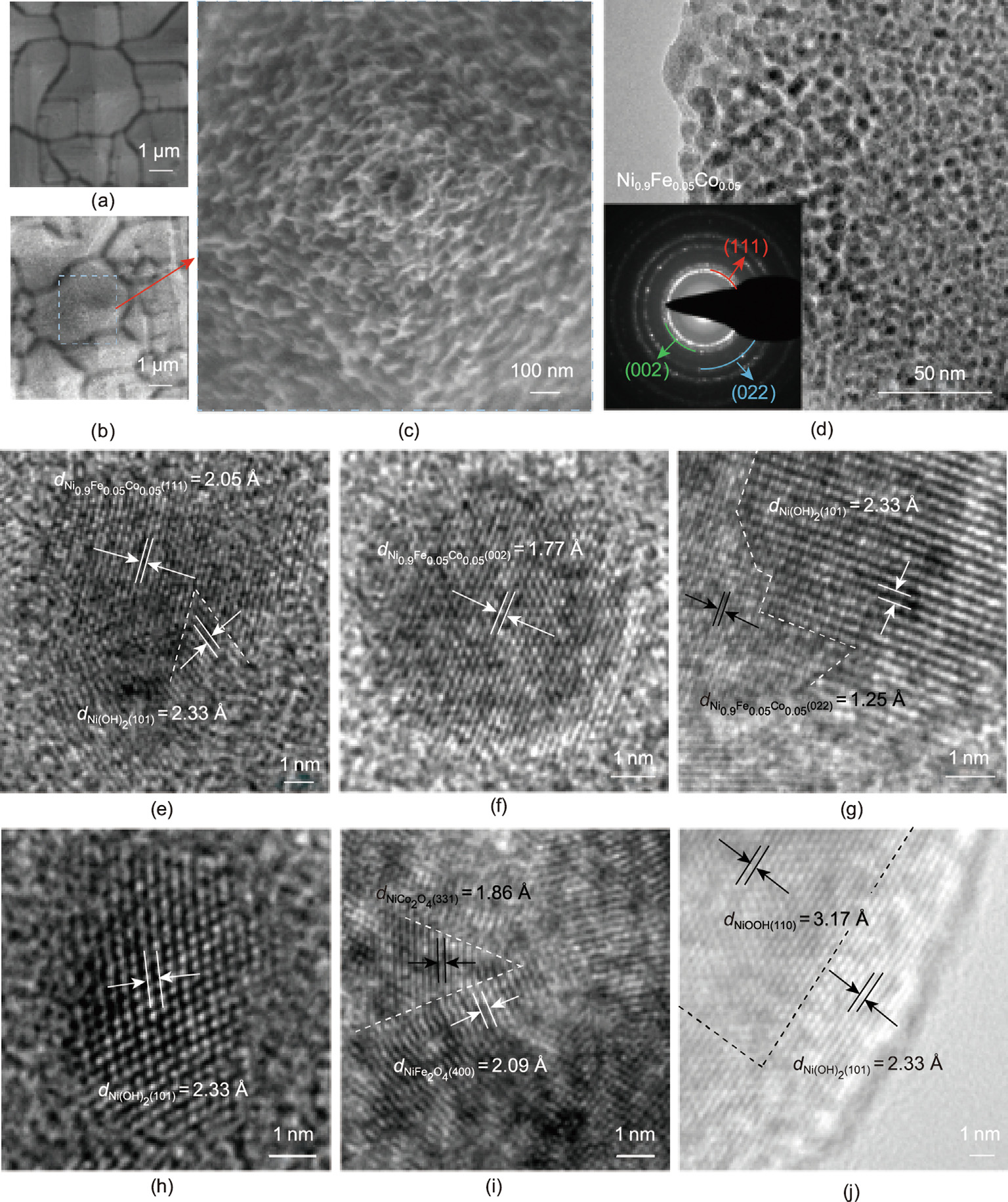
Fig. 2. SEM and TEM images of the Ni0.9Fe0.05Co0.05 protective layer deposited on the p+n-Si photoanode. (a) SEM image of the p+n-Si substrate; (b, c) SEM images of the Ni0.9Fe0.05Co0.05 protective layer coated on the p+n-Si substrate; (d) TEM image of the Ni0.9Fe0.05Co0.05 protective layer on the p+n-Si substrate (inset, selected area electron diffraction (SAED) pattern); (e–j) high-resolution TEM (HRTEM) images in different regions of the Ni0.9Fe0.05Co0.05 protective layer coated on the p+n-Si substrate.
The PEC performance of the Ni0.9Fe0.05Co0.05/p+n-Si photoanode was evaluated using a three-electrode configuration in 1.0 mol∙L–1 NaOH electrolyte under AM 1.5G simulated solar illumination without current–resistance (IR) correction (ohmic potential loss for correcting). The Ni/p+n-Si and Ni0.9Fe0.1/p+n-Si photoanodes were tested as references under the same conditions (Fig. 3(a)). In comparison with the Ni/p+n-Si photoanode, which exhibited a Von of about 1.06 V versus RHE and a Jph of about (14.9 ± 0.2) mA∙cm–2, the Ni0.9Fe0.1/p+n-Si photoanode exhibited enhanced PEC activity with a Von cathodically shifted to about 1.0 V versus RHE and a Jph reaching about (25.2 ± 0.2) mA∙cm–2. With the simultaneous introduction of Fe and Co, the Ni0.9Fe0.05Co0.05/p+n-Si photoanode showed an outstanding PEC performance, with a Von further cathodically shifted to 0.938 V versus RHE and a Jph increased to be as high as (33.1 ± 0.2) mA∙cm–2.
《Fig. 3》

Fig. 3. PEC performances of the obtained photoanodes in 1.0 mol∙L–1 NaOH solution without IR correction (ohmic potential loss for correcting). (a) CV curves of the obtained photoanodes under simulated solar illumination and the Ni0.9Fe0.05Co0.05/p+-Si electrode in the dark (E0 OER is the theoretical potential for water oxidation). (b) Amounts of collected H2 and O2 gases and the Faradaic efficiency of the Ni0.9Fe0.05Co0.05/p+n-Si photoanode (solid lines: calculated H2 (light blue triangle) and O2 (pink triangle) amounts; dotted lines: measured H2 (blue semi-circle) and O2 (red semi-circle) amounts; calculated Faradaic efficiencies of H2 (blue semi-square) and O2 (red semi-square) products). The Faradaic efficiency is the ratio of the measured gas amounts to the calculated gas amounts. (c) Applied bias photon-to-current efficiency (ABPE) of the obtained photoanodes. (d) Stability measurement of the Ni0.9Fe0.05Co0.05/p+n-Si photoanode under simulated solar illumination.
As an important metric, the photovoltage—defined here as the potential difference between the n-Si-based photoanode and the p+ -Si-based electrode when reaching a current density of 10 mA∙cm–2 under solar light and in the dark [38]—was determined to be 527 mV for the Ni0.9Fe0.05Co0.05/p+n-Si photoanode. Such a large photovoltage indicates that the formed Ni0.9Fe0.05Co0.05/p+n-Si junction can effectively drive the water oxidation reaction. It is also noteworthy that the Ni0.9Fe0.05Co0.05/p+ -Si electrode displayed excellent electrocatalytic OER activity in the dark, with an anodic current density of 10 mA∙cm–2 being achieved at about 1.54 V versus RHE, which actually outperforms the benchmark IrO2/C and NiFe/glassy carbon (GC) electrodes [39,40]. This finding confirms that the Ni0.9Fe0.05Co0.05 layer acts as an admirable OER catalyst that can effectively accelerate the water oxidation kinetics.
Next, to obtain the real applied bias photon-to-current efficiency (ABPE) of the Ni0.9Fe0.05Co0.05/p+n-Si photoanode (0.25 cm2 ), it was essential to calculate the Faradaic efficiencies for hydrogen and oxygen evolution. Here, the oxygen (O2) and hydrogen (H2) production rates were measured to be 82.75 and 162.04 μmol∙h–1, respectively (Fig. 3(b); Table S1 in Appendix A). Given the theoretical production rates of O2 (84.37 μmol∙h–1) and H2 (168.73 μmol∙h–1) determined using Coulomb’s law, the Faradaic efficiencies were calculated to be approximately 98% for oxygen evolution and 96% for hydrogen generation. Thus, the maximum ABPE of the Ni0.9Fe0.05Co0.05/p+n-Si photoanode was 3.20% at about 1.08 V versus RHE for oxygen evolution, which is 5.0 and 2.2 times that of the Ni/p+n-Si (0.65% at ~1.15 V vs RHE) and Ni0.9Fe0.1/p+n-Si (1.47% at ~1.13 V vs RHE) photoanodes (Fig. 3(c)), respectively. These comparative results confirm that the trimetallic Ni0.9Fe0.05Co0.05 layer efficiently catalyzes the OER, endowing the Ni0.9Fe0.05Co0.05/p+n-Si photoanode with an outstanding PEC activity that is superior to those of most n-Si-based photoanodes used for water oxidation (Table S2 in Appendix A).
The PEC stability was also considered as a key evaluation indicator for the photoanodes. As shown in Fig. 3(d), the Ni0.9Fe0.05Co0.05/p+n-Si photoanode exhibited outstanding stability, with a photocurrent density well maintained at about (34.1 ± 1.5) mA∙cm–2 at 1.6 V versus RHE during approximately 41 h PEC reaction. The slightly reduced photocurrent density could be recovered after removing the bubbles covering the photoanode or by using fresh 1.0 mol∙L–1 NaOH electrolyte after a long operation time. After being stored at room temperature and air pressure for 6 months, the Ni0.9Fe0.05Co0.05/p+n-Si photoanode still exhibited excellent PEC performance with very slight degeneration (Fig. S8 in Appendix A). These results demonstrate that the Ni0.9Fe0.05Co0.05 protective layer stabilizes the p+n-Si photoanode for PEC water oxidation by effectively preventing surface corrosion in an aqueous alkaline electrolyte.
As described in the following sections, the interfacial properties of these p+n-Si-based photoanodes were systematically investigated to unravel the underlying mechanisms for the improved PEC performance. As shown in Fig. 4(a), Mott–Shottky (M–S) plots were collected for the Ni/p+n-Si, Ni0.9Fe0.1/p+n-Si, and Ni0.9Fe0.05Co0.05/p+n-Si photoanodes in the dark. It is well known that the point where the tangent of the near-linear regional curve intersects the x-axis in an M–S diagram is regarded as the flat-band potential (Efb) of the semiconductor material [41,42]. It is noticeable that the similar Efbs of the Ni0.9Fe0.05Co0.05/p+n-Si (0.06 V vs RHE) and Ni0.9Fe0.1/p+n-Si (0.07 V vs RHE) photoanodes are more negative than that of the Ni/p+n-Si (0.18 V vs RHE) photoanode. As further shown in the XPS valence band (VB) spectra (Fig. S9 in Appendix A), the VB edge of the Ni0.9Fe0.05Co0.05 layer is close to that of the Ni0.9Fe0.1 layer, which is much higher than that of the Ni layer. These findings reveal that, due to the incorporation of Fe, a larger band bending is generated at the Ni0.9Fe0.05Co0.05/p+n-Si and Ni0.9Fe0.1/p+n-Si interfaces, relative to that at the Ni/p+n-Si interface, which accelerates the interfacial charge transfer by producing a larger driving force.
《Fig. 4》

Fig. 4. (a) Mott–Shottky (M–S) plots for the Ni/p+n-Si (green), Ni0.9Fe0.1/p+n-Si (blue), and Ni0.9Fe0.05Co0.05/p+n-Si (red) photoanodes in 1.0 mol∙L–1 NaOH electrolyte in the dark (CSC is the capacitance of the space-charge layer). (b) Capacitive currents at 1.1 V versus RHE as a function of CV scan rates for the Ni/p+-Si (green), Ni0.9Fe0.1/p+-Si (blue), and Ni0.9Fe0.05Co0.05/p+-Si (red) electrodes. (c) Nyquist plots for the Ni/p+n-Si (green), Ni0.9Fe0.1/p+n-Si (blue), and Ni0.9Fe0.05Co0.05/p+n-Si (red) photoanodes under simulated solar illumination in 1.0 mol∙L–1 NaOH at 1.0 V versus RHE. Inset: equivalent circuit model. RS: resistance of the external circuits, including the pure electrolyte, circuit wire, and contact resistance between the work photoanode and wire; RSC1: resistance of charge transfer at the metallic layer/p+ n-Si interface; RSC2: resistance of interfacial charge transfer at the metallic layer/electrolyte interface; Q1 and Q2: constant phase element. (d) Charge injection efficiency uinj (solid line and solid sphere) and charge separation efficiency usep (dashed line) of the Ni/p+n-Si (green), Ni0.9Fe0.1/p+n-Si (blue), and Ni0.9Fe0.05Co0.05/p+n-Si (red) photoanodes under simulated solar illumination.
To clarify the population of electrochemically active sites at the metallic layer/electrolyte interface, the electrochemically active surface areas (ECSAs) of the different electrodes were determined using the double-layer capacitance (CDL) [43] calculated from the CV curves [44,45]. Given that CDL was determined to be 4.35, 1.59, and 1.11 mF∙cm–2 for Ni0.9Fe0.05Co0.05/p+ -Si, Ni0.9Fe0.1/p+ -Si, and Ni/p+ -Si, respectively (Fig. S10 in Appendix A; Fig. 4(b)), the ECSA was calculated to increase from 27.75 for Ni/p+ -Si to 39.75 for Ni0.9Fe0.1/p+ -Si, and then dramatically increase to 108.75 for Ni0.9Fe0.05Co0.05/p+ -Si. These comparative results again indicate that the introduction of Fe and Co, especially Co, results in the production of plenty of catalytically active sites exposed at the surface that efficiently drive the water oxidation reaction, as was previously revealed by the XPS analysis.
To investigate the interfacial electrochemistry, electrochemical impedance spectroscopy (EIS) measurements of the p+n-Si-based photoanodes (0.25 cm2 ) were carried out under simulated solar illumination in 1.0 mol∙L–1 NaOH at 1.0 V versus RHE (Fig. 4(c)). Upon fitting with the equivalent circuit model (Fig. 4(c), inset; Table S3 in Appendix A) [46], the Nyquist plots display very close interfacial resistance (RSC1) at the Ni0.9Fe0.1/p+ -Si interface (6.7 Ω) and the Ni0.9Fe0.05Co0.05/p+n-Si interface (6.8 Ω), which is much smaller than that at the Ni/p+n-Si interface (12.0 Ω). It can then be supposed that the introduction of Fe reduces the interface electrical resistance and then promotes charge separation at the metallic layer/p+n-Si interface. This deduction is well explained by the large band bending at the metallic layer/p+n-Si interface (see the analysis of M–S plots (Fig. 4(a)) and XPS VB spectra (Fig. S9 in Appendix A)), effectively driving the interfacial charge transfer. In addition, with the incorporation of Fe and Co, a greatly decreased charge transfer resistance (RSC2) is observed at the photoanode/ electrolyte interface for the Ni0.9Fe0.05Co0.05/p+n-Si photoanode (11.6 Ω), as compared with the Ni0.9Fe0.1/p+n-Si (91.0 Ω) and Ni/p+n-Si (1592.0 Ω) photoanodes. This result implies significantly accelerated charge transfer and hole injection processes at the photoanode/electrolyte interface for the Ni0.9Fe0.05Co0.05/p+n-Si photoanode, which can be attributed to the simultaneous incorporation of Fe and Co, producing plenty of electrochemically active sites for the water oxidation reaction, as is well supported by the ECSA analysis.
In order to further understand the charge separation and transfer processes at the internal interface of the photoanode and at the photoanode/electrolyte interface, the photogenerated charge separation efficiency (φsep) and injection efficiency (φinj) were measured and calculated (Fig. S11 in Appendix A; Fig. 4(d)) [47,48]. As shown in Fig. 4(d), the φsep at 1.23 V versus RHE increased from 35.5% for Ni/p+n-Si to 72.2% for Ni0.9Fe0.1/p+n-Si and then to 77.8% for Ni0.9Fe0.05Co0.05/p+n-Si, which suggests that the introduction of Fe and Co inhibits the charge recombination at the metallic layer/ p+n-Si interface. In particular, the introduction of Fe provides the greatest contribution to the increased φsep at the metallic layer/ p+n-Si interface for the promoted charge separation. It should also be noted that, in comparison with the Ni/p+n-Si photoanode, which possesses a relatively low φinj of about 61.7% at 1.23 V versus RHE, the φinj is increased to 79.5% for Ni0.9Fe0.1/p+n-Si and further to 90.3% for Ni0.9Fe0.05Co0.05/p+n-Si. This impressive increase in φinj suggests that photoholes are effectively injected into the electrolyte and then become involved in the water oxidation reaction, which can be attributed to the introduction of Fe and Co creating more electrocatalytically active sites, as previously evidenced by the ECSA results. Then, the facilitated hole transfer processes from the photoanode to the electrolyte enable a great improvement in the PEC water oxidation activity for the Ni0.9Fe0.05Co0.05/p+n-Si photoanode.
As shown in the above analysis of the electronic structures and electrochemical properties, the introduction of Fe and Co into the Ni metallic layer not only regulates the band bending at the metallic layer/p+n-Si interface to promote interfacial charge separation but also creates abundant electrocatalytically active sites to accelerate the water oxidation reaction kinetics, thereby synergistically contributing to the excellent PEC performance of the Ni0.9Fe0.05Co0.05/p+n-Si photoanode. To further investigate the effects of the incorporation of Fe and Co on the thermodynamics of the water oxidation reaction at the photoanode/electrolyte interface, molecular dynamics (MD) simulations and firstprinciples density functional theory (DFT) calculations were carried out. Structural models with the interaction between water and the catalyst surface reproduced by MD simulations (Fig. S12 in Appendix A) were constructed for DFT calculations on the four-electron reaction pathways of water oxidation at the Ni, Ni0.9Fe0.1, and Ni0.9Fe0.05Co0.05 layers (Table S4 in Appendix A and Figs. 5(a)–(c)). Fig. 5(d) shows the reaction free energy diagrams and the rate-limiting steps for water oxidation [39], with the calculated Gibbs free energies of each reaction step ( , eV) and the OER overpotential (η, V) listed in Table S4.
For the Ni layer, the thermodynamically rate-determining step (RDS) is the third step, that is, *O→*OOH (Fig. 5(a)), which must overcome a free energy barrier of  = 2.22 eV. The corresponding overpotential (η) of the OER process is determined to be 0.99 V. With the introduction of Fe, the *O→*OOH step remains as the RDS for the Ni0.9Fe0.1 layer (Fig. 5(b)), while is significantly reduced to 2.01 eV, with a much lowered η of 0.78 V required for the OER. Remarkably, with the incorporation of both Fe and Co, is further reduced to 1.43 eV, with the fourth step (i.e., *OOH→O2) acting as the RDS for the Ni0.9Fe0.05Co0.05 layer (Fig.5(c)). Given the free energy barrier of the fourth step (
 = 1.81 eV), the corresponding η is calculated to be as low as 0.58 V. It is theoretically demonstrated that the electron cloud overlap between the *O species and the surface atoms for Ni0.9Fe0.05Co0.05 (where the calculated value of the iso-surface is 0.068 electrons per cubic angstrom (e∙Å–3 )) is significantly weakened (Figs. 5(e) and (f)), indicating a weaker bond interaction between the Ni and O atoms [49], in comparison with that for Ni0.9Fe0.1 (where the calculated value of the iso-surface is 0.071 e∙Å–3 ). Thus, the energy required for the third step occurring at the surface of the Ni0.9Fe0.05Co0.05 is decreased, resulting in a change in the RDS from *O→*OOH to *OOH→O2 for water oxidation. In accordance with the previous experimental results, these theoretical calculations also reveal that the modulation of the electronic structures by the incorporation of Fe and Co thermodynamically benefits the water oxidation reaction at the surface of the deposited Ni0.9Fe0.05Co0.05 layer.
《Fig. 5》
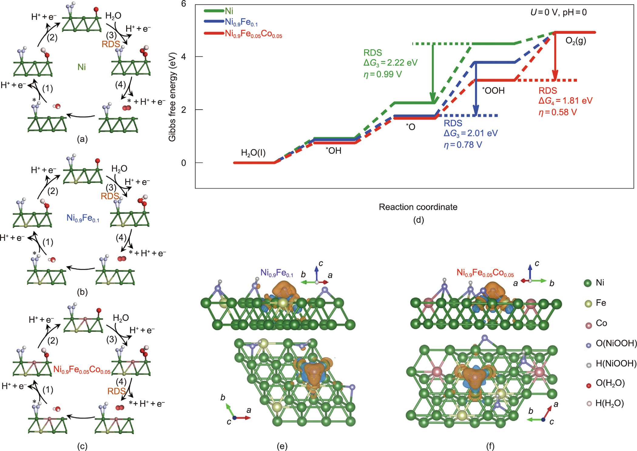
Fig. 5. (a–c) Reaction pathways of water oxidation with *, *O, *OH, and *OOH (where * represents the active sites, and *O, *OH, and *OOH represent the adsorbed intermediates) for the (a) Ni, (b) Ni0.9Fe0.1, and (c) Ni0.9Fe0.05Co0.05 layer. (d) Gibbs free energy diagrams for the deposited Ni, Ni0.9Fe0.1, and Ni0.9Fe0.05Co0.05 layers (U= 0 V, pH = 0, U is the applied electrode potential vs standard hydrogen electrode). (e, f) Side and top views of the charge density differences in the deposited (e) Ni0.9Fe0.1 and (f) Ni0.9Fe0.05Co0.05 layer. Cyan and orange regions represent electron accumulation and depletion, respectively. RDS: rate-determining step.
As shown in Fig. 6(a), upon simulated solar illumination, holes and electrons are produced in the p+n-Si substrate, while the metal (hydr)oxides formed in situ at the surface of the UPD-deposited metallic layers serve as effective electrocatalysts for water oxidation. The introduction of Fe increases the band bending at the metallic layer/p+ n-Si interface, which produces a large photovoltage (~527 mV for Ni0.9Fe0.05Co0.05/p+n-Si) to accelerate the interfacial charge separation. The incorporation of Fe and Co triggers an evolution of the electronic structure in the deposited metallic layers, introducing abundant Ni3+ species and Ov in the Ni0.9Fe0.05Co0.05 layer, which act as electrochemically active sites to facilitate water oxidation kinetics. Hence, the UPD-deposited Ni0.9Fe0.05Co0.05 protective layer effectively catalyzes and stabilizes the p+n-Si photoanode for efficient PEC water splitting.
Having obtained a high-performance Ni0.9Fe0.05Co0.05/p+n-Si photoanode, we then fabricated a PV/PEC device by coupling the Ni0.9Fe0.05Co0.05/p+n-Si photoanode with cheap Si solar cells for unassisted solar-driven water splitting (Fig. 6(b)). In a twoelectrode system with platinum (Pt) plate as the cathode, the Ni0.9Fe0.05Co0.05/p+n-Si photoanode exhibited a Von of 0.982 V and a photocurrent density of about 18.2 mA∙cm–2 at 1.23 V (Fig. S13 in Appendix A). To optimize the configuration of the PV/PEC device, different series-connected (SC) Si solar cells (Fig. S14 in Appendix A) were combined with the Ni0.9Fe0.05Co0.05/p+n-Si photoanode and the Pt cathode. It was noted that a photocurrent of 14.8 mA at a voltage of 1.19 V was obtained by the intersection of the two photocurrent–voltage (J–V) curves, which is higher than that of a commercial RuIr/Ti mesh electrode (3 cm × 4 cm; detailed information provided in Fig. S15 in Appendix A) and PV curves (6.8 mA at 1.54 V; detailed information provided in Fig. S16 in Appendix A). As shown in Fig. 6(c), with 3-SC Si solar cell providing an open circuit voltage (Voc) of about 1.71 V and a solar-to-electric power conversion efficiency of about 20%, the fabricated PV/PEC device (PV: ~1 cm2 , PEC: 0.51 cm2 ) produced a high photocurrent reaching 14.8 mA without bias, and an STH efficiency calculated to be approximately 12.0%, which is superior to almost all the Sibased PV/PEC devices reported in the previous literature (Table S5 in Appendix A). In addition, the PV/PEC device exhibited quite good stability, with the photocurrent and STH being well maintained at (15.0 ± 0.2) mA and about 12.0%, respectively, over 20 h continuous operation for unassisted solar water splitting (Fig. 6(d)).
《Fig. 6》

Fig. 6. (a) Schematics of PEC water splitting over the Ni0.9Fe0.05Co0.05/p+n-Si photoanode. (b) Schematics of the PV/PEC device (PV: Si solar cell; PEC: Ni0.9Fe0.05Co0.05/p+n-Si photoanode). (c) Linear sweep voltammetry curve and the calculated STH of the PV/PEC device without external bias under simulated solar illumination (operating current of the PV/PEC device: 14.8 mA). (d) Photocurrent (black line) and corresponding STH (red line) of the assembled PV/PEC device for unassisted solar water splitting depending on the proceeding reaction.
To realize the future application of solar water splitting, largearea photoanodes should be prepared to integrate PV/PEC devices. Moreover, the performance of the PV/PEC device should be evaluated under simulated solar light with different illumination intensities, considering the different light intensities of the sun at different times. It should be noted that the presence of numerous generated gas bubbles can cover the photoanode surface and thereby hinder the water oxidation reaction under high-intensity illumination or at a large-area photoanode. Bubble generation and growth processes at micro-/nano-textured photoelectrodes should be seriously considered in order to optimize the configuration and operation of PV/PEC devices for excellent solar water splitting performance.
《3. Conclusions》
3. Conclusions
In summary, a trimetallic NiFeCo protective layer was successfully deposited on a p+n-Si substrate by UPD to stabilize and catalyze PEC water splitting. In comparison with p+n-Si photoanodes coated with monometallic (Ni) or bimetallic (NiFe) layers, the optimized NiFeCo/p+n-Si photoanode exhibited a greatly increased PEC performance under simulated solar illumination, with an onset potential of about 0.938 V versus RHE and a photocurrent density of about 33.1 mA∙cm–2 at 1.23 V versus RHE, contributing to a high ABPE of 3.2%. It was demonstrated that the introduction of Fe mainly regulates the band structure at the NiFeCo/p+n-Si interface, yielding a large band bending to promote interfacial charge separation, while the introduction of Co modulates the electronic structure at the surface of the NiFeCo layer, providing abundant catalytically active sites to accelerate the water oxidation kinetics, which synergistically enhances the PEC activity of the NiFeCo/p+nSi photoanode. In addition, an assembled PV/PEC device (PV: Si solar cell; PEC: the optimized NiFeCo/p+n-Si photoanode) achieved an STH conversion efficiency of 12.0% for unassisted solar-driven water splitting. This work not only presents a deep understanding of the structure–activity relationship for designing efficient Sibased photoanodes but also provides an attractive approach to configurate simple and cheap PV/PEC devices driven by inexpensive Si solar cells for unassisted solar-driven water splitting.
《Acknowledgments》
Acknowledgments
This work was supported by the Basic Science Center Program for Ordered Energy Conversion of the National Natural Science Foundation of China (51888103). Shaohua Shen is grateful to the National Natural Science Foundation of China (52225606), the Fundamental Research Funds for the Central Universities, and the Youth Innovation Team of Shaanxi Universities.
《Authors’ contributions》
Authors’ contributions
Lingyun He and Zhonghang Xing carried out the photoanode synthesis, characterizations, and photoelectrochemical measurements. Lingyun He, Jiafeng Geng, and Jinzhan Su fabricated the PV/PEC device and conducted relative performance tests. Lingyun He and Shaohua Shen wrote the paper. Xin Hong and Yiqing Wang conducted the DFT calculations. Penghui Guo helped with the XPS measurements and analysis. Shaohua Shen conceived the idea and supervised the project. All the authors discussed the results and commented on the manuscript.
《Compliance with ethics guidelines》
Compliance with ethics guidelines
Lingyun He, Xin Hong, Yiqing Wang, Zhonghang Xing, Jiafeng Geng, Penghui Guo, Jinzhan Su, and Shaohua Shen declare that they have no conflict of interest or financial conflicts to disclose.
《Appendix A. Supplementary data》
Appendix A. Supplementary data
Supplementary data to this article can be found online at https://doi.org/10.1016/j.eng.2022.03.023.


 京公网安备 11010502051620号


