
《1. Introduction》
1. Introduction
In the past decade, artificial intelligence (AI), with the widespread use of deep learning, has achieved great success in various fields such as machine vision [1], autonomous driving [2], playing board games [3,4], and clinical diagnosis [5,6]. Despite rapid developments of AI in theories and applications [7], the computing power required to train or execute state-of-the-art AI models increases much faster than the development of integrated electronic circuits characterized by the well-known Moore’s law, which seems to be slowing [8]. Vast quantities of data are generated every second from enormous numbers of sensors and internet-connected devices with an explosive growth rate in the coming fifth generation mobile communication technology (5G) era. These data are required to be processed by AI as fast as possible. Neural networks, a representative AI model composed of multiple layers of neurons with thousands or millions of interconnections to learn representations of data with multilevel abstractions, are becoming increasingly complicated. As the current AI models have sufficient performance for many applications, they have recently met another fundamental bottleneck for their future development in computing hardware in terms of speed and power consumption [9,10].
To solve this generally recognized problem, various efforts have been conducted in recent years in innovations of electronic architectures to accelerate AI inference and training at low power consumption [11,12]. For example, application-specific integrated circuits (ASICs) have been widely accepted in industry by eliminating unnecessary operations [13]. Brain-inspired (neuromorphic) computing mimics the working principle of the brain with colocations of both the memory and processor, which can solve the well-known ‘memory wall’ problem in traditional Von Neumann architecture, leading to extremely high power efficiency [14]. Both spiking neural networks (SNNs) [14] and memristive crossbar arrays [15] have recently shown great potential for inmemory computing with integrated chips. However, these methods still rely on electronic components whose speed and energy are fundamentally limited by Joule heating, capacitance, and radio frequency (RF) crosstalk [16].
Optical computing provides another solution by harnessing the unique properties of light [17,18]. As light has a much broader bandwidth, the information can be highly parallelized at different wavelengths with almost no crosstalk between adjacent channels [19,20]. Other dimensions such as polarization and orbit angular moments can also be explored to further increase the bandwidth [21,22]. With the data or weight encoded in different wavelengths by an optical frequency comb, the operation at a single time step can be inherently applied to thousands or millions of channels simultaneously. In addition, the modulation of light can be conducted in the phase domain with low power consumption [23]. The development of fibers and waveguides causes extremely low loss for light to propagate a long distance at unparalleled light speeds [24]. All these factors make photons more attractive than electrons as information carriers, except for the difficulty of manipulation. Telecommunication is a typical example, as the data can be transferred with a much larger throughput by optical fibers than by traditional electric cables at lower consumptions. Moreover, it has become increasingly popular to apply chip-tochip optical interconnections in cloud computing due to the high bandwidth density [25].
Although optical computing also has a long history with various pioneering architectures [26–29], it remains a great challenge to apply photons for computing with performance comparable to that of state-of-the-art electronic processors in previous decades, mainly due to the lack of suitable integrated architectures and integrated photonics devices including efficient and high-speed opto-electro modulators [30,31], detectors [32], low-power optical frequency combs [33], and nonlinear nonvolatile optical materials [34]. While recent developments of various integrated photonics devices and novel materials, together with the rise of AI, seem to provide a great opportunity for the renaissance of optical computing, different kinds of optical neural networks and photonics processors have been proposed recently to address the computing power bottleneck of AI. This research is more practical than ever, as we do not need to replace electronic computers totally but strive to find an entry point for optical computing in specific tasks or operations. Perhaps a hybrid optoelectronic framework can facilitate complementation of both electrons and photons with orders of magnitude improvement in AI-specific applications [35], working as the transitory stage for all-optical computers in the future.
Therefore, AI-specific optical computing is a relatively young field but has become very popular and competitive in the past five years, with large developments occurring in almost every aspect. Since the development of integrated photonics processors definitely requires multidisciplinary efforts, it is necessary to gather an increasing number of people in this exciting area. Here, we provide a brief review of the recent breakthroughs of analog optical computing in different AI models with their unique strengths in solving versatile applications and remaining challenges for practical implementations. The remainder of this review is arranged by different mainstream AI models. Section 2 focuses on the forward optical neural network, with a description of different optical methods for different mathematical operations involved. Section 3 describes the optical reservoir computing and Section 4 briefly introduces other AI models. Finally, in Section 5, we summarize several important challenges remaining to be solved.
《2. Feedforward optical neural network (ONN)》
2. Feedforward optical neural network (ONN)
In a feedforward artificial neural network, all the neurons in neighboring layers are interconnected with different synaptic weights. For each neuron, a linear weighted summation operation is first performed. It is assumed that there are a total of N incoming signals conveyed from the previous layer, denoted by a column vector x =  (where
  is the Nth signal intensity; N is the total number of incoming signals; T is matrix transpose). The corresponding weighting coefficients are denoted by another row vector w =
  (where
  is the Nth weighting coefficient; N is the total number of weighting coefficients). The linear summation result for this individual neuron is
  , which further triggers a nonlinear activation function
  . The final output of this neuron is
  . If we consider all M neurons in the same layer, then the entire linear operation is a vector–matrix multiplication,
  , where
  refers to a vector consisting of M linear weighted summation results for different neurons and
  refers to a M × N matrix consisting of all the weighting coefficients. Compared to the electronic implementation of artificial neural networks, optical implementation can support intrinsic parallel calculations at the speed of light with a lower energy cost [36–38].
《2.1. Optical linear weighted summation》
2.1. Optical linear weighted summation
For the optical implementation of a fully connected neural network, it is necessary to optically perform a weighted summation operation or a vector–matrix multiplication operation. To date, there have been several experimental realizations of optical weighted summation as follows.
2.1.1. Cascaded Mach–Zehnder interferometers (MZIs)
In this scheme [36,39–50], the input and output vectors are represented by multiple coherent light signal intensities at different ports. They are connected by a mesh of cascaded MZIs, which serve as the optical computing device for vector-matrix multiplication. The basic concept of cascaded MZIs dates back to early work in 1994 [39], and a programmable nanophotonic processor containing 56 MZIs in a silicon photonic integrated circuit was presented in recent work [36].
In mathematics, a general real-valued matrix can be decomposed as  by singular value decomposition (SVD), where U and V are both unitary matrices with sizes M × M and N × N, respectively, and
  is a M × N rectangular nonnegative real-valued diagonal matrix. Both U and V can be optically implemented by a mesh of MZIs, and can be implemented by optical attenuators. As the basic unit in this system, a MZI has two beam splitters and two tunable phase shifters, as shown in Fig. 1 [47]. It should be noted that a MZI is not equivalent to a neuron in an artificial neural network, but a mesh of MZIs can jointly perform the same linear vector-matrix multiplication operation between two layers of neurons in a network. In the design of a MZI mesh, the interconnection topology of all the MZIs and the phaseshifting angle for each phase shifter need to be optimized. For a typical cascaded MZI system, a N × N matrix multiplication requires at least N (N – 1) =2 beam splitters [41]. The method of constructing a MZI mesh is not unique for the vector-matrix calculation [41,42]. For example, two different MZI meshes can be designed for the same vector-matrix calculation, with features of either being more tunable or being more fault tolerant [42]. The susceptibility of the MZI mesh to fabrication errors and imprecisions for practical imperfect photonic components has been investigated [42,43]. With three-dimension (3D) printed photonic waveguides, a system of cascaded MZIs can be extended from twodimension (2D) to 3D to achieve higher computational capabilities [44,45]. Complex-valued computing operations can also be implemented efficiently with this architecture [46]. Cascaded MZIs have been attempted for various artificial intelligent tasks such as vowel recognition [36], flower data classification [47], and wine data classification [47].
《Fig. 1》
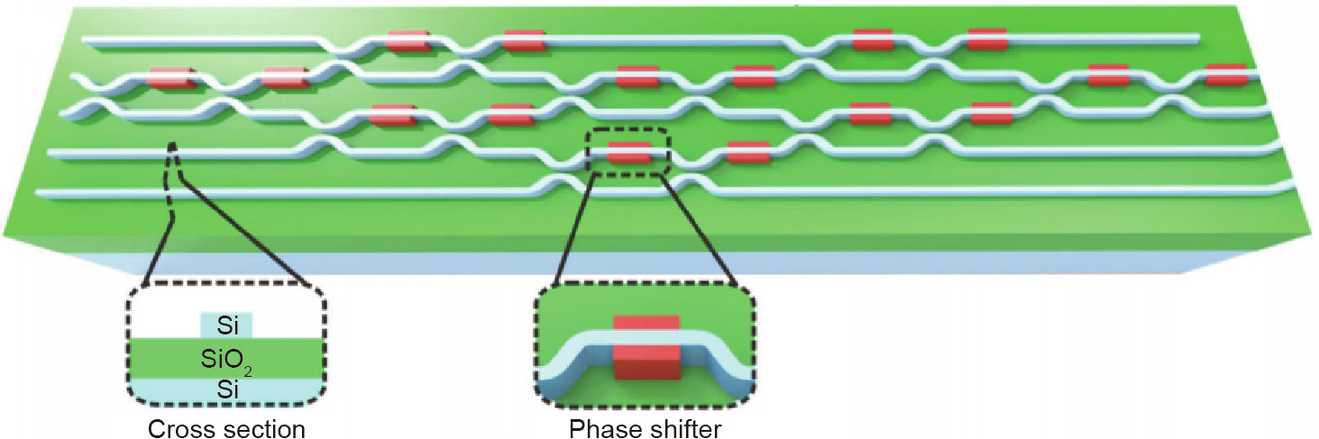
Fig. 1. A system of cascaded MZIs for linear vector-matrix multiplication (Si: silicon material; SiO2: silicon dioxide material). Reproduced from Ref. [47] with permission of The Optical Society of America, ©2019.
2.1.2. Deep diffractive neural network (D2NN)
In the D2NN architecture [51], multiple layers of cascaded diffractive optical elements (DOEs) are placed perpendicular to the light propagation direction with certain space separation, as shown in Fig. 2 [51]. The spatial light intensity distributions in the input and output planes correspond to the input and output vectors, respectively. The incident light field propagates forward in free space and it is sequentially modulated by each DOE. The pixel values (phase-only, amplitude-only, or complex-amplitude) of all the DOEs are optimized by an error backpropagation algorithm similar to the counterpart in deep learning. The entire optimized system performs a linear transform from the input light field to the output light field to realize vector-matrix multiplication. The information processing capacity of a D2NN system depends on the number of diffractive layers [52]. This architecture can be used as a linear classifier and has been proven to be able to optically classify number digit images in the MNIST dataset and fashion product images in the Fashion-MNIST dataset with moderately high accuracy [51]. The D2NN architecture has been improved from different aspects in later works [53–68]. The original D2NN was driven by a terahertz source, and a more compact system with an infrared source is presented in Ref. [53]. The implementation of D2NN is not limited to monochromatic coherent light illumination, and a broadband D2NN can be realized for spectral filtering and wavelength demultiplexing applications [54]. D2NN can be combined with a digital processor [55–57] or a digital neural network [58] to improve the inference performance. A residual D2NN architecture is also proposed, analogous to the residual deep learning network, and the direct shortcut connection between the input and output is optically implemented simply with multiple reflecting mirrors [59]. Lensless free-space propagation can be replaced with an optical Fourier transform with a lens to improve the prediction accuracy [60]. The shift-, rotation-, and scale-invariant recognition capability of a D2NN system can be enhanced by geometrically transforming the training images [61]. Simulation results show that a D2NN system can solve more diversified computer vision tasks such as image segmentation [60], salience detection [60] and image superresolution [59], as well as object classification [51].
《Fig. 2》
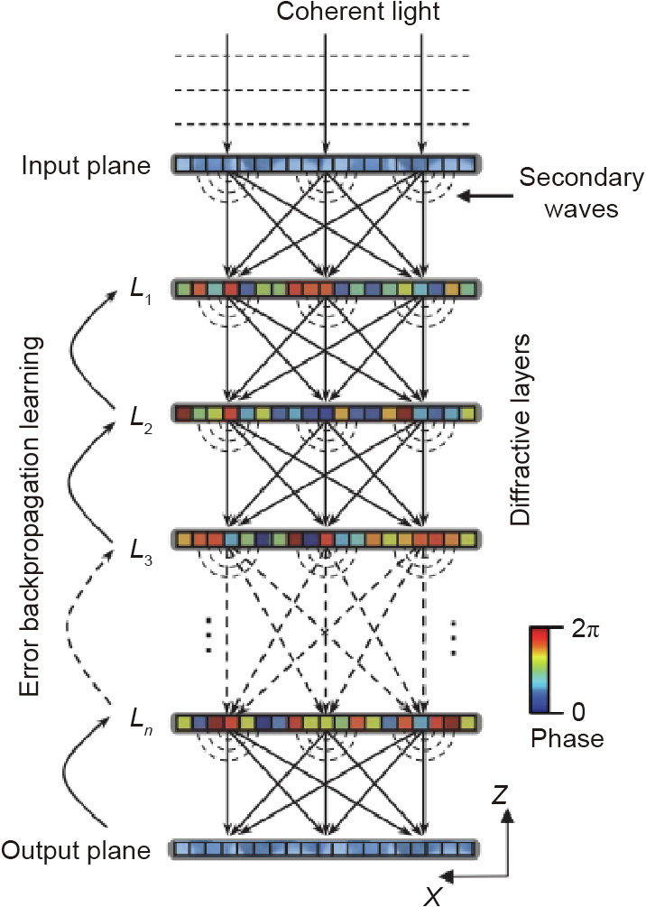
Fig. 2. Optical system of D2NN. L1, L2, L3, and Ln: first, second, third and nth diffractive layer. Reproduced from Ref. [51] with permission of The American Association for the Advancement of Science, ©2018.
In addition to conventional machine learning tasks, D2NN can be applied to other optical computing and optical signal processing tasks including intelligent beam steering for lidar [62], image encryption [63], optical logic gates [64], pulse shaping [65], and mode recognition/multiplexing/demultiplexing in mode-division optical fiber communication [66–68].
2.1.3. Spatial light modulator (SLM) and lens-based optical computing
Unlike the previous two architectures designed for coherent light, this architecture based on a SLM and lens can work with both coherent and incoherent light illumination [69–74]. The intensity distribution of incident light illuminating different pixels (or portions) of a SLM plane carries input vector values. Different pixels of the SLM are encoded according to the weighting coefficients. The SLM is placed at the back focal plane of the lens, and the light converges to the focal point. A detector placed in the focal point of the lens then collects the total light intensity on the SLM plane as the inner product between the input vector and weighting coefficient vector. This architecture shown in Fig. 3(a) is similar to the single-pixel imaging (or ghost imaging) concept in optical imaging [70,71].
《Fig. 3》
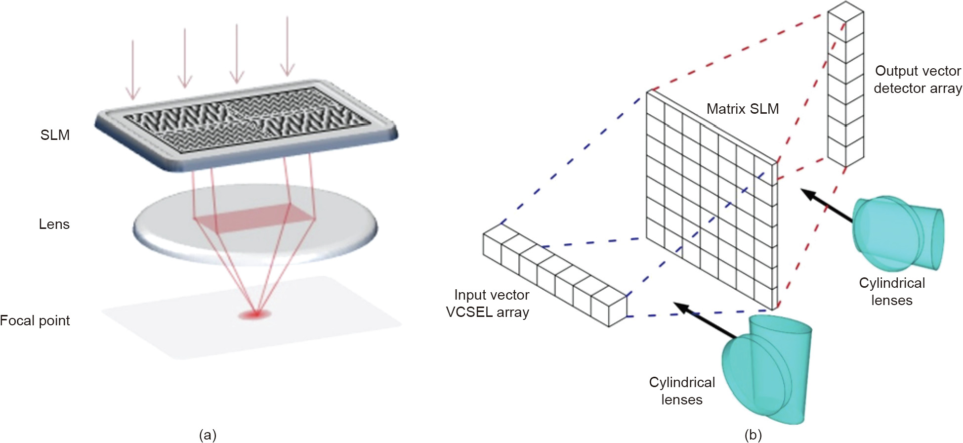
Fig. 3. (a) Linear weighted summation operation with SLM and a Fourier lens; (b) vector-matrix multiplication with SLM and cylindrical lenses [74]. (a) Reproduced from Ref. [69] with permission of The Optical Society of America, ©2019.
By using different types of lenses, there are many ways to realize complete vector matrix multiplication. Typically, one can use a Fourier lens to realize the summation of the output lights along the same direction, and the different focal points for parallel lights along different directions correspond to the different elements of the output vectors [69]. An alternative is to use the cylindrical lens [73,74]. A cylindrical lens only performs a transformation between parallel light and converged light in either the horizontal direction or vertical direction. The input vector is represented by the light intensity distribution along a horizontal pixelated array. Two cylindrical lenses perform a fanout of a one-dimensional input array and a one-dimensional weighted summation on the SLM plane, as shown in Fig. 3(b) [74]. Finally, the multiplication result is represented by the light intensity distribution along a vertical array in the output focal plane. In addition, vector matrix multiplication can be implemented by simply repeating the weighted summation operation multiple times with a single Fourier lens.
The SLM- and lens-based architecture can be easily combined with cold atom systems to realize an all-optical deep neural network with both linear and nonlinear transformations [69,72]. It is feasible to build a large-scale programmable all-optical deep neural network with 174 optical neurons based on this architecture [72]. Compared to other architectures, this implementation is fully reprogrammable for different tasks without changing the physical setup.
2.1.4. Wavelength division multiplexing (WDM)
In this approach [34,75–81], linear weighted summation is realized in a WDM manner. Each element in the input vector is represented by a light wave with a unique frequency (or wavelength), which then undergoes different spectral filtering by photonic weight banks usually constructed by microring resonators (MRRs); hence, the input signals are weighted, as shown in Fig. 4 [75]. A balanced photodiode (BPD) collects the total light power of all the signals in different wavebands to realize the weighted linear summation. This architecture is considered to be potentially compatible with the mainstream silicon photonic device platform. A simplified feedback control method for microring weight banks to produce favorable filtering responses is proposed in Ref. [78]. The MRR control method can be improved to be compatible with large-scale photonic integrated circuits [80]. This architecture has been used in principal component analysis [81]. In recent works [19,38,82], the WDM architecture has been combined with photonic chip-based microfrequency combs, which can significantly increase the data processing speed and capacity. Nonvolatile phase changing materials (PCMs) are integrated onto waveguides to locally store weighting values on chip [38]. The optical vector convolutional accelerator in Ref. [82] can perform more than ten trillion operations per second.
《Fig. 4》
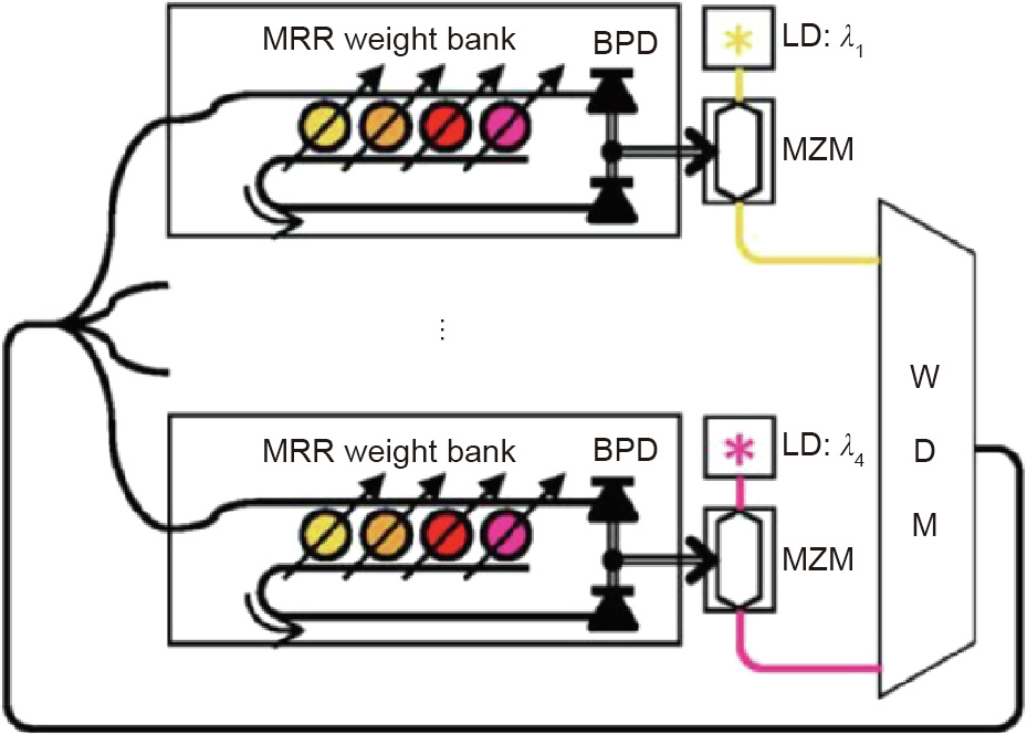
Fig. 4. Optical computing with WDM and MRR.  : wavelength for the first and fourth MRR weight bank; LD: laser diode; MZM: Mach-Zehnder modulator. Reproduced from Ref. [75] with permission of Springer Nature, ©2017.
2.1.5. Other implementations
Vector-matrix multiplication can also be implemented based on light propagation through a nanophotonic medium, as shown in Fig. 5 [83]. The input light intensity distribution entering the medium denotes the input image pattern. The output intensity distribution after the light field passes the medium denotes the computational result, such as image classification result. The medium consists of host materials and inclusion materials with different indices, and the inclusion materials can more strongly scatter light. With the locations and shapes of inclusions appropriately optimized, the light field inside the medium can be scattered as designed to realize vector multiplication with the weight matrix. In a more recent work [84], to reduce the design complexity, the continuous medium was replaced with multiple layers of metasurfaces with optimized ribbon sizes.
《Fig. 5》
Fig. 5. Nanophotonic medium with inclusions for optical computing. Gray: host material, white: inclusions. Reproduced from Ref. [83] with permission of China Laser Press, ©2019.
In an architecture based on a coherent matrix multiplier [85], both the input vector and weighting values are encoded as multiple channels of coherent light signals. Linear weighted summation is implemented by the quantum photoelectric multiplication process in homodyne detectors. The coherent matrix multiplier has some potential advantages for implementing a large-scale and rapidly reprogrammable photonic neural network.
Furthermore, an ONN can be realized inside a multicore optic fiber. Each input, output, and weighting value is represented by the light intensity in each individual core inside a multicore fiber. The weighting cores are doped with erbium and serve as controlled amplifiers. Optical signals are transferred transversely between cores by means of optical coupling to mimic forward signal propagation in a neural network. The simulation results show that a three-layer neural network can be constructed by a multicore fiber in Refs. [86,87].
《2.2. Optical linear convolution》
2.2. Optical linear convolution
Compared with a fully connected neural network, the neurons are connected more sparsely in a convolutional neural network (CNN). In addition, the same weight values are shared by multiple connections. The vector-matrix multiplication operation between the neurons in two neighboring neuron layers is essentially a convolution operation.
Mathematically, the convolution between an input image and a kernel is equivalent to Fourier filtering of the input image. In optics, the Fourier transform and inverse Fourier transform of an input light field containing the image information can be easily implemented by a 4f double-lens setup. A filtering mask designed according to the convolution kernel can be placed in the Fourier plane of the 4f setup. Previous works [37,88–90] demonstrate that such an optical convolution operation can significantly reduce the computational cost in a CNN. A generalized photonics tensor operation processor to perform convolution in the Fourier domain is further implemented in Ref. [91]. Alternatively, the convolution operation can be implemented in other ways such as cascaded acousto-optical modulator arrays [92], wavelength-division multiplexing plus optical delay lines [93] or dispersion-induced delay [82], and 3D printed photonic waveguide circuits [44].
《2.3. Optical nonlinear activation function》
2.3. Optical nonlinear activation function
If a neural network is fully linear without any nonlinear activation function, there could be physically multiple layers of linear transformations, but the effective computation is always equivalent to one layer since the multiplication results of multiple matrices is still one single matrix. To realize an all-optical deep neural network, the implementation of a nonlinear activation function is indispensable. Unfortunately, nonlinear behavior in optics is not easily implemented experimentally, which makes the realization of a feasible nonlinear activation function one of the most challenging issues in ONN research. In many ONN studies, only the linear operation is implemented optically, and the nonlinear operation is usually simulated [36,37,58,60,89,94].
In general, the nonlinear activation function can be implemented as a hybrid system composed of both electronic components and optical components [36,55,56,95,96], but this approach inevitably slows down the performance of optical computations due to the mutual conversion between optical and electronic signals. The ideal scenario is to realize nonlinear activation functions using pure optical elements, which was recently demonstrated to be possible by using electromagnetically induced transparency (EIT) [69,72].
EIT is a coherent optical nonlinearity in a medium in which the transparency of one light is controlled by another light, as shown in Fig. 6 [69]. Theoretically, EIT can happen in any real material system with triplets of states, where the transition probability amplitude between different states depends on their particle populations. In Refs. [69,72], Zuo et al. used cold atom systems in a two-dimensional magneto-optical trap. The authors combined the linear transformation using SLM and a lens and the nonlinear activation functions using EIT to construct a complete all-ONN and used it to classify different phases of the Ising model.
《Fig. 6》
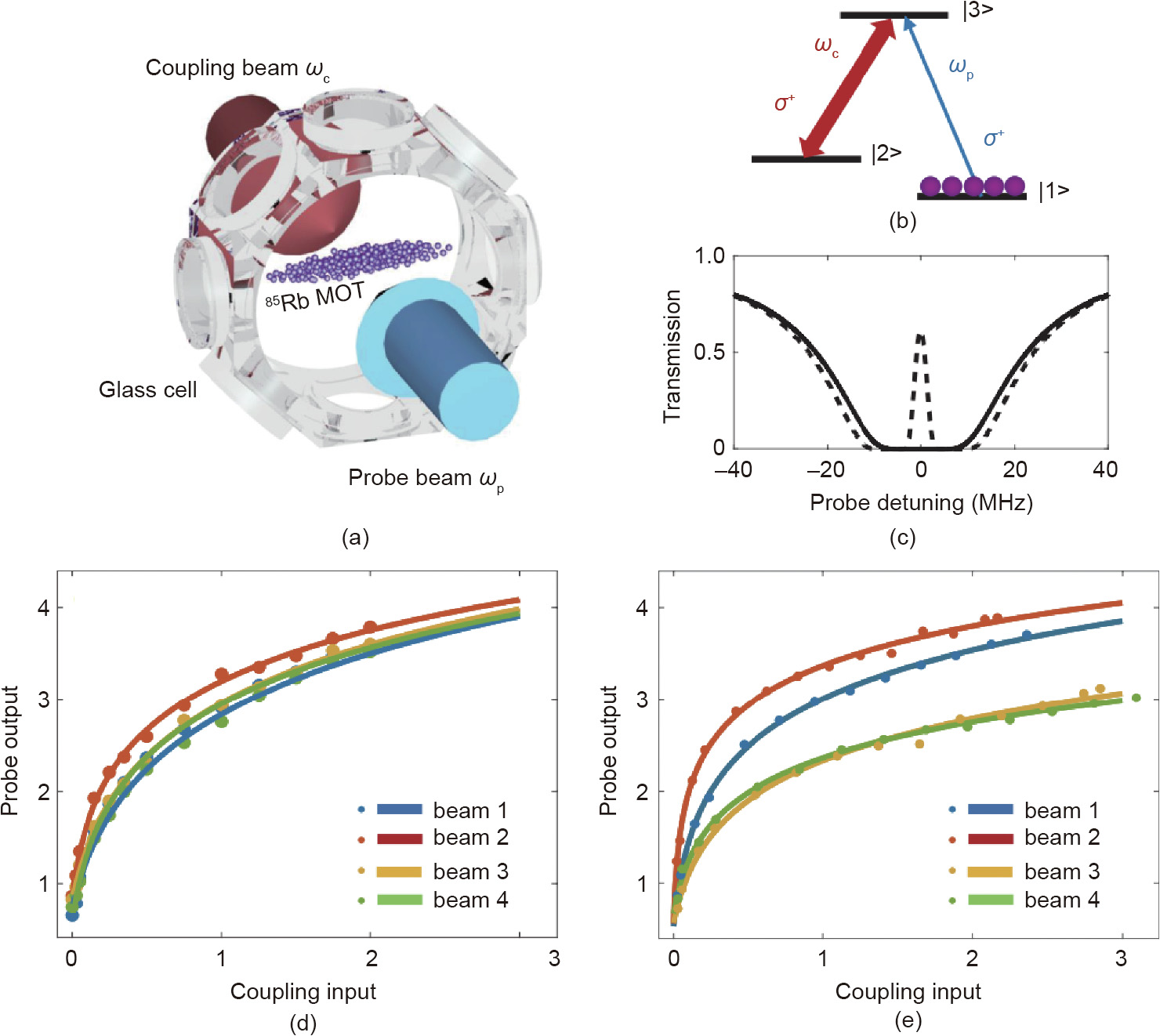
Fig. 6. Nonlinear activation functions were realized using EIT. ωc : frequency of coupling beam; ωp: frequency of probe beam; σ+: circularly polarized light. Reproduced from Ref. [69] with permission of The Optical Society of America, ©2019.
In addition, there are other approaches [94] such as reverse saturated absorption (RSA) to realize the nonlinear activation function, but so far, none of them has been proven to be feasible in experiments.
《2.4. In situ optical training》
2.4. In situ optical training
A deep learning network is usually first trained by a large number of samples to optimize all the weighting coefficients. After the network is trained, it can perform a certain inference task efficiently for testing samples. In many ONN works, such as in Refs. [36,51], the training is conducted fully digitally offline on a computer, and only the inference operation of the ONN is performed optically. However, the challenge of in situ training of an ONN has been addressed to a certain extent.
The in situ training of a MZI mesh has been investigated in several works [36,47,48]. Error backpropagation is the most widely used training algorithm for a digital neural network. Adjoint variable methods are used to derive the photonic analog of the backpropagation algorithm for a mesh of MZIs [48]. In the training, the gradients in the calculation can be measured by the light intensities at different nodes of the MZI mesh. Alternatively, a forward propagation and finite difference method without backpropagation can be used for the on-chip training of a system of cascaded MZIs [36].
Two neuroevolutionary algorithms, the genetic algorithm and particle swarm optimization, are proposed to optimize the parameters of a MZI mesh for in situ training [47]. These global optimization algorithms are gradient-free and can avoid the local minimum problem.
For the D2NN architecture, an in situ training method has also been investigated [56]. The standard training algorithm for DNNs is based on error backpropagation, and the in situ gradients are obtained by measuring the forward and backward propagated optical fields based on light reciprocity and phase conjunction principles. Each layer of static DOE is replaced with an SLM for dynamic training and updating of parameters. The residual error between the actual output light field and the target light field is generated from a complex field generation module (CFGM) for light field propagation in the inverse direction. The simulation results show that this in situ training scheme can save significant computational cost compared with offline computer training.
For other ONN architectures, on-chip in situ training can be realized if proper optimization algorithms, accurate experimental measurements and dynamically encoded optical elements are available.
《3. Optical reservoir computing (RC)》
3. Optical reservoir computing (RC)
RC is a type of neuromorphic computing framework derived from the recurrent neural network that allows for fast learning and easy implementations with various hardware systems. Because of its special advantage in processing temporal data, this architecture has shown optimum results when performing timedependent tasks, such as sequential signal prediction and voice recognition. A RC structure is generally composed of a fixed nonlinear mechanism, such as reservoir nodes, which allows the input signal to be transformed into spatiotemporal states in a higherdimensional space. The temporal output data of the reservoir are obtained by training a reservoir state reader to determine the reservoir dynamics. This section reviews the all-optical and optoelectronic implementation of RC on integrated optical circuits or developed by spatial optical diffraction.
《3.1. All-optical RC》
3.1. All-optical RC
The difference between all-optical and optoelectronic implementations of RC depends on the different types of reservoirs and input layers. In the following, we introduce the all-optical structure from spatially distributed RC to delay-based RC. Ultrahigh-speed computation and low power consumption are the main advantages of an all-optical RC system.
3.1.1. Spatially distributed RC based on diffractive coupling
Spatially distributed photonic RC is suggested as one method of RC implementation by utilizing a DOE. In 2015, Brunner and Fischer [97] introduced a network of vertical-cavity surfaceemitting lasers (VCSELs). Fig. 7 shows a chip from Princeton Optronics [97].
The RC architecture has shown the realization of laser coupling and diffractive multiplexing by the DOE. Fig. 7 shows the experimental implementation, which introduces the structure of an image consisting of VCSEL. Here, the combination of the VCSEL array lattice spacing and the focal length of the imaging lens can form an angle between the chief rays of adjacent lasers, which can be adjusted by the focal length of the lens.
《Fig. 7》

Fig. 7. (a) VCSEL laser diode array and (b) Coupling between lasers by implementing the designed diffractive resonator. d1: image distance; d2: object distance;  : wavelength; φ: angular offset; κDOE: the efficiency of DOE; POL: polarizer. Reproduced from Ref. [97] with permission of The Optical Society of America, ©2015.
Due to the inherent manufacturing process, the lasers located on the array are affected by parameter changes throughout the laser integrated circuits. Therefore, the demonstrated diffractive coupling with a periodic DOE is susceptible to such differences. In addition to network coupling, diffraction imaging allows parallel optical modulation of multiple lasers, and the primary restriction on laser coupling is determined by optical aberration from the image. The structure has shown considerable scalability [98,99], which is expandable to a network composed of hundreds of nodes placed with an area less than 1 mm2 . For technically relevant implementations, the miniaturization of the introduced method must first be declared. In particular, a concentration on wavelength uniformity is required because of the phenomena of injection locking [100].
3.1.2. Delay-based RC
To simplify the intricate hardware of photonic systems, Appeltant et al. [99] and Paquot et al. [101] introduced a novel type of RC, which is delay line-based RC. They combined a feedback structure divided into a series of virtual nodes and only one nonlinear node together in a circle to form delayed feedback. Compared with spatially distributed RC with high network degrees of freedom, these kinds of reservoirs are fixed, which allows more traditionally used optical communication hardware. The diagram of delay linebased RC is shown in Fig. 8(a) [99], and in the following, we demonstrate two typical delays in line-based RC.
《Fig. 8》
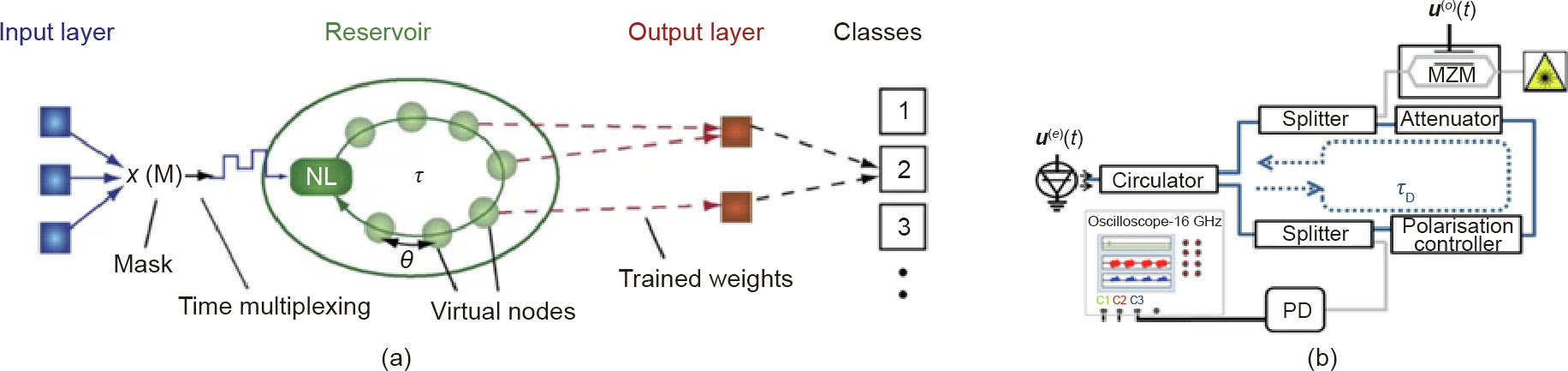
Fig. 8. (a) Scheme of delay line-based RC. The delay loop, which is divided by many intervals, forms the reservoir. The reservoir contains virtual nodes along the delay line. (b) Scheme of a reservoir based on a semiconductor laser; it utilizes a series of optical devices to establish RC. NL: nonlinear element; τ: the delay in the feedback loop; PD: photo diode;  : electrical information input;
  : optical information input; τD: feedback delay. (a) Reproduced from Ref. [99] with permission of Springer Nature, ©2011; (b) Reproduced from Ref. [102] with permission of Springer Nature, ©2013.
We first discuss the first type of delay-based RC with optical inputs to an all-optical reservoir. This kind of RC contains several implementations based on semiconductor lasers [102], semiconductor optical amplifiers (SOAs) [103], or passive optical cavities [104]. Duport et al. [103] and Brunner et al. [102] utilized active devices to introduce two different types of nonlinear responses, a SOA and a semiconductor laser. A modulated optical field was injected into the input, and after detection, they utilized the output layer. This RC paradigm has the potential for complicated tasks for computation. Moreover, the optical reservoir is able to process information at a relatively high rate of Gbytes. Fig. 8(b) shows the schematic of this system [102]. The external input layer injected through the semiconductor and optical feedback can be used to form an optical reservoir. According to Hicke et al. [105] and Nakayama et al. [106], their method can improve the processing ability.
Moreover, the delay-based optical reservoir can be implemented onto a chip. Nguimdo et al. [107] demonstrated that the necessary optical bias injection can increase the optical modulation bandwidth of semiconductor lasers, allowing shorter delay times than that of the system of Brunner et al. [102]. An on-chip semiconductor ring laser subject to optical feedback can be used to solve two different tasks simultaneously, such as a classification task and a time series prediction task [108]. The bandwidth of a semiconductor laser can be increased by the bias injection method of Nguimdo et al. [107] to formulate a shorter delay time than that of the system of Brunner et al. [102]. The classification and prediction task [108] can be solved by an on-chip semiconductor laser based on optical feedback. If the readout layer is slightly modified[106], using short external cavities could avoid phase sensitivity [109]. It is indispensable for passive devices to develop lowconsumption and high-efficiency photonic computers. Dejonckheere et al. placed a semiconductor saturable absorber mirror (SESAM) in a ring-like optical cavity [110]. Vinckier et al. [104] demonstrated photonic RC subject to a kind of coherently driven passive cavity. If we conduct a nonlinear output in the reservoir computer, utilizing linear fiber cavities becomes possible, and they can easily perform tasks such as digit recognition based on voice information.
《3.2. Optoelectronic RC》
3.2. Optoelectronic RC
RC based on optoelectronic systems has been widely used and performed marvelously in several fields, such as voice recognition [111–113], chaotic temporal prediction [111,114,115], and radar signal forecasting [116,117]. The processing speed of present optoelectronic RC has realized megahertz speed and has, in the foreseeable future, potential to develop gigahertz speed [118].
3.2.1. RC at the chip-scale
In 2008, Vandoorne et al. [119] declared the first RC on hardware based on silicon-on-insulator, consisting of waveguides, optical combiners, and optical splitters. Researchers have found that detection through standard fast photodiodes can solve the problem of nonlinearity. However, since this system relies on photoelectric conversion in the detector, it cannot be fully optically operated [119–121].
The advantages of using passive components are their wide bandwidth, and it is even possible to send several wavelengths into the system synchronously, thereby realizing a parallel operating system of discrete wavelengths. New learning techniques can be used to adapt to long-term phase drift. One of the disadvantages is that as the chip expands to more nodes, the increased optical loss may be considerable, and it is difficult to realize a parallel measurement of all nodes. In a passive component network, the frequency of the input signal clock and memory timescale is dependent on the propagation delay between separated nodes, which would request a high injection frequency of up to hundreds of Gbit/s [122].
The estimation of RC’s computing property is measured through various tasks. For this reason, researchers have simplified the random input connectivity in the software RC by injecting the photonic signal into the reservoir at one point. When processing longer time-series data, a larger chip is necessary. As shown in Fig. 9, the experimental results have shown digital values only, which can be constructed as an integrated filter [122]. In experiments and the digital implementation of the system, several further tasks, such as recognition of voice digits, still need to be assessed. In all tests, the system produced sufficient results. Moreover, optoelectronic implementation Ikeda-like ring optical cavities [123,124] can be implemented on silicon chips to construct delay-based RC. Larger et al. [111] (Fig. 10(a)) and Paquot et al. [112] developed this kind of optoelectronic implementation of RC separately.
《Fig. 9》
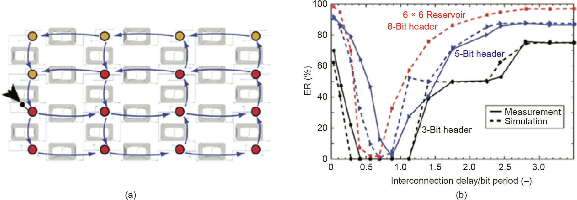
Fig. 9. Reservoir based on a passive silicon chip. ER: error rate; ‘‘-” represents the previous bit number. Reproduced from Ref. [122] with permission of Springer Nature, ©2014.
The input and output layers of most hardware implementations of optoelectronic RC are emulated offline on a standard computer, where the computer simulates most of the input and output layers in RC implementations on hardware. Single reservoir computers with optoelectronic devices, however, have been established by implementing the three layers of RC on analog hardware [116]. The input layer can be implemented by a mask with two different sinusoidal frequencies. A dual-output Mach-Zehnder modulator (MZM) obtains the signal from the optical reservoir, and an RLC filter filters the signal that the BPD outputs, as shown in Fig. 10(b) [116]. The output of the whole analog system becomes the terminal output of the reservoir computer. Fig. 10(b) shows the readout layer.
《Fig. 10》
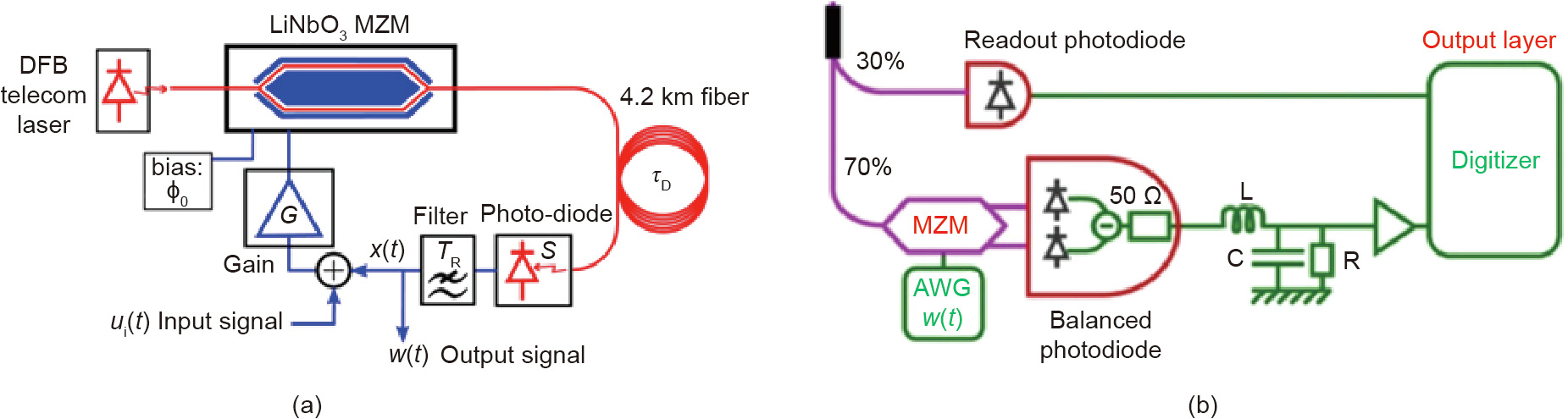
Fig. 10. (a) Scheme of the optoelectronic reservoir computer. The optical path is depicted in red and the electronic is depicted in blue. (b) Scheme of the analog readout layer. DFB: distributed feedback-based; x(t): delayed signal; τD: delay time; w(t): continuous time weight function; AWG: arbitrary waveform generator; R, L, C: resistor, inductor, and capacitor. (a) Reproduced from Ref. [111] with permission of The Optical Society of America, ©2012; (b) Reproduced from Ref. [116] with permission of Springer Nature, ©2016.
Although training the readout weights of delay RC has seldom been considered, Antonik et al. [125] proposed using fieldprogrammable gate arrays (FPGAs) as dedicated hardware for a novel access to train the weights online. This optoelectronic implementation has been favorably applied to neural information processing [125] and emulating chaotic systems [126]. FPGAs can process information at a speed of hundreds of megahertz. Moreover, traditional training algorithms such as genetic and gradient descent algorithms can be utilized in the online training discussed above. Additionally, multiple delays can be implemented to increase the performance of photonic delay RC [113,127,128].
3.2.2. Free-space optical RC
Another method of RC photonic realization is using the excitability of special optical components. Neuromorphic excitable photonic devices based on the spike model can be realized using semiconductor technology [77,129–132,133]. Therefore, the network of this excitable nanophotonic device was achieved similarly to neuromorphic inspiration, which brings very favorable power consumption [134]. A laser is transformed as an excited system, such as a spike, as the optical power increases above a stable threshold. In 2016, Shastri et al. [132] accomplished a digital experiment with two excitable lasers. They evaluated a larger network based on the electro-optical excitation of semiconductor lasers [135]. To facilitate numerous nodes on one chip, the system is constructed based on WDM technology. In 2011, Barbay et al. [129] established another structure, which is the excitable neuron-like pulse behavior of a monolithic semiconductor micropillar laser. The structure has a refractory period [136]. Microring and disk lasers have also shown optical excitability [133,134]. Compared with the previous design, the mechanism of these synchronized laser devices has replaced the saturable absorber and shown internal symmetry breaking characteristics. To date, the latest developments indicate that photonics can achieve SNNs with incomparable speed.
Recently, a new method based on the spatially scalable photonic library of digital micromirror devices (DMD) and SLM has been presented [137–141]. In 2018, Bueno et al. [137] proved that an optical system with SLM, DOE, and camera could store a network of up to 2500 diffraction coupled photon nodes. By modulating the intensity of light in a binary way, Dong et al. [138] encoded the input information and the reservoir with DMDs. Later, they applied the same method using phase-only SLM to obtain a large-scale optical reservoir network [139]. Input and reservoir information can be introduced by the reservoir network with the assistance of the spatial phase distributions. In 2020, Rafayelyan et al. [140] showed that strong scattering media play a key role in optical networks to guarantee stochastic coupling weights among the numerous photonic nodes as well as parallel processing in the network. Prediction tasks in multidimensional large chaotic systems have been demonstrated in their large system with excellent accuracy and achieved a relatively high speed with low power consumption. The proposed network has demonstrated the potential scalability and capability of processing larger datasets.
《3.3. Outlook》
3.3. Outlook
With the appearance of the architecture of combined nanophotonics and RC, a new way of processing photonic information is leading the field. The low power consumption and ultrafast speed represent relative advantages over traditional methods. For the potential future development of photonic RC, ultrahigh-speed optical nonlinearities and optical devices with ultralow power consumption may lead to a bright future in the field, which can greatly increase the reservoir performance in terms of speed and power efficiency [142,143]. Additionally, the scalability of the photonic chip with a multi-node reservoir is required for research in the future.
《4. Spiking neural network》
4. Spiking neural network
《4.1. Recent development》
4.1. Recent development
SNNs are proposed as an interdisciplinary topic of biology and neuroscience [144]. Compared with feedforward neural networks and recurrent neural networks, SNNs are more widely used in neuromorphic computing. In addition to the meta model, neurons in SNNs are activated only when their membrane potential reaches the threshold. When a neuron is activated, a signal is generated and transmitted to modify the membrane potential of the cascading neurons. In SNNs, the current activation level of the neuron is usually modeled as a certain differential equation. The level rises after the arrival of the stimulation spiking and continues for a period of time and then declines gradually.
SNNs enhance the ability to process spatiotemporal data. On the one hand, neurons in SNNs are only connected to nearby neurons and processed separately to enhance the ability to process spatial information. On the other hand, since the training relies on the spiking interval, information lost in the binary code can be retrieved from time information of the spiking, thereby increasing the ability to process temporal information. Facts have demonstrated that spiking neurons are better computing units than traditional artificial neurons. Nevertheless, due to difficulties in the training and physical implementation of SNNs, they have not yet been widely used. Most of the research works on SNNs still focus on theoretical analysis and the verification of simple structures. However, more researchers are now engaged in training algorithms and hardware (optical) implementation of SNNs.
In 2016, Princeton University’s Prucnal research group proposed a spiking processing system based on an activatable graphene fiber laser [132]. The system contains an erbium-doped fiber (gain part), a graphene saturated absorber (loss part) with a 980 nm laser acting as a pump source, and a 1480 nm laser carrying a spiking stimulation signal to excite the system to generate a leaky integrate-and-fire spiking neuron response. In 2018, the research team proposed a distributed feedback-based (DFB) laser-structured neuromorphic photonic integrated circuit [145]. In addition, the research team discussed the feasible scheme of constructing programmable and cascadable photonic neural networks, including broadcast-and-weight network prototypes [132] and coherent optical schemes. Among them, the broadcast-and-weight network prototype is a network architecture that can support the parallel interconnection of large-scale photon spiking neurons. The training method of SNNs mainly follows supervised learning algorithms. These supervised learning algorithms include ① the SpikeProp algorithm [146], which utilizes gradient descent and is usually employed for multilayer feedforward artificial neural networks; ② the Tempotron algorithm [147], which changes the network weights using the difference between the spiking sequence output and the expected sequence; ③ synaptic plasticity-based algorithms such as the Hebbian learning algorithm [148–152]; ④ remote supervised learning algorithms such as the ReSuMe algorithm [149]; and ⑤ supervised learning algorithms based on spiking sequence convolution, such as the SPAN algorithm [150] and PSD algorithm [151]. There are also supervised and unsupervised learning algorithms that are based on VCSELs [152] and use vertical-cavity semiconductor optical amplifiers (VCSOAs) for STDP implementation [153].
In 2019, Feldmann et al. [34] proposed another scheme based on PCM and adopted this scheme to perform nonlinear transformations for photonic neurons. Light-controlled PCM is a type of working state. The working state of the material between crystalline and amorphous materials is controlled by the input optical power. When the input optical power becomes lower than the threshold, the PCM is in the crystal state, and a large amount of optical power is absorbed. When the input optical power becomes higher than the threshold, the PCM is in an amorphous state, and most of the optical power passes through it. Therefore, integrating the material into the optical transmission medium can change the optical permeability of the material according to the input optical power. In this way, it is capable of working as the activation function of the photonic neuron.
《4.2. Comparison between neuromorphic photonics and electronics》
4.2. Comparison between neuromorphic photonics and electronics
Compared with the neuromorphic electronics implementation of SNNs, such as TrueNorth [154], Neurogrid [155], and SpiNNaker [156], neuromorphic photonics process information using light that enables much higher bandwidths and data throughput as well as lower latencies. It has been shown that the optoelectronic SNN using a hybrid silicon/III-V platform achieves a 20 GHz processing rate, which is over six orders of magnitude higher than that of a pure electronic SNN [157]. Since the energy is mainly consumed by the laser source and the passive filters have a low leakage current, the energy efficiency of the hybrid silicon/III-V platform is 0.26 pJ per operation, which is approximately three orders of magnitude higher than that of Neurogrid and is over six orders of magnitude higher than that of SpiNNaker. The computing performance of neuromorphic photonic platforms can be further improved by using optimized subwavelength structures (e.g., photonic crystals) and wavelength multiplexing.
《5. Conclusions》
5. Conclusions
While optical computing has been widely exploited in different AI models, its practical application with significantly better performance than that of traditional electronic processors has still not been demonstrated due to various challenges. For example, how can strong optical nonlinear properties be obtained with a short response time and low requirement for the power of the probe light? How can the nonlinear characterization be optimized in different architectures? How can high-speed large-scale reconfigurability be achieved on chips with low power? How can different photonics devices be integrated on a single chip, especially with peripheral units? How can an ONN be designed with automation software for different tasks? Despite many problems remaining to be solved in the future, current techniques of analog optical computing have already shown the unique potential of light in terms of speed, data parallelization, and power consumption [158].
For the next step, we think more efforts needs to be invested to address key shortcomings of light and demonstrate the superiority of optical computing over electronic computing in different practical applications. Different architectures, as described before, may be suitable for very specific tasks with their unique characters. A more accurate and efficient model to describe the propagation and modulation of partially coherent light fields in free-space optical computing may facilitate high-speed data processing in computer vision. Because most of the light in natural scenes such as autonomous driving is incoherent, it is difficult to apply the coherent model in current diffractive neural networks. As nonlinear properties play a key role in deep neural networks, a better strategy to realize nonlinear activation functions by optics with low power and short response time can significantly improve the accuracy of the current ONN. Memory and access are fundamental technologies required to scale up neuromorphic processors. However, it has long been a challenge to construct optical random access memory with extremely fast read and write speed, which provides a great opportunity for the development of specific materials for optical computing and storage. Despite the use of bulky systems, free-space optical computing may accelerate cloud computing in various data centers that do not require portable systems. We expect more advanced SLMs with a high refreshing speed up to MHz and for giga-scale pixel numbers. High-speed low-power photoelectric conversion is increasingly important at the current transitory stage, requiring both photons and electrons for practical applications. All challenges and applications indicate an increasing number of breakthroughs in the near future [159].
In summary, we have reviewed the developments of optical computing for AI-specific hardware implementations mostly in the last five years. We describe the unique strengths of different architectures regarding several representative AI models. Although most methods are still at the stage of proof-of-concept systems, we expect the future development of these frameworks for practical applications with orders-of-magnitude improvement in either speed or power efficiency. With increasing efforts from different fields including photonics, electronics, materials, fabrications, computer science, and biology, we believe that hybrid optoelectronic computers to accelerate AI training and inference will come soon as a transitory stage toward all-optical computers for general applications.
《Acknowledgements》
Acknowledgements
This work was supported by the National Natural Science Foundation of China (61927802, 61722209, and 61805145), the Beijing Municipal Science and Technology Commission (Z1811000 03118014), and the National Key Research and Development Program of China (2020AAA0130000). J.W. acknowledges the support from the National Postdoctoral Program for Innovative Talent and Shuimu Tsinghua Scholar Program. J. L acknowledges the support from the Hong Kong Research Grants Council (16306220).
《Compliance with ethics guidelines》
Compliance with ethics guidelines
Jiamin Wu, Xing Lin, Yuchen Guo, Junwei Liu, Lu Fang, Shuming Jiao, and Qionghai Dai declare that they have no conflict of interest or financial conflicts to disclose.


 京公网安备 11010502051620号


