

《1. Introduction》
1. Introduction
Wireless communication systems, which have evolved from the first generation in the 1980s to the most recent fifth generation (5G), have been a driving force enabling the technology that has changed the world in terms of communications and our daily lives. We are now connected anytime and almost anywhere via wireless networks, with access to a vast amount of real-time information. However, the 5G system, which has a peak data rate of around 10 gigabits per second (Gbps), is still insufficient for some applications (e.g., holograms and multi-sense communications, which are the next frontiers in the virtual mode of communication), and researchers around the world have started to work on the next generation—that is, the sixth generation (6G) wireless system— with an expected data rate of more than 1 terabit per second (Tbps), as shown in Fig. 1 [1–3]. A number of white papers have recently been published by organizations such as the International Telecommunication Union (ITU) Network 2030 and the IMT-2030 (6G) Promotion Group in China [4], suggesting that the operational frequency band will be moved from the current microwave and millimeter-wave (mmWave) to the terahertz (THz) frequency band for future wireless systems in order to meet the high data rate and bandwidth requirements. It is envisaged that 6G wireless technologies may integrate the Internet of Things (IoT) to cover a very wide range of applications (e.g., healthcare, autonomous systems, and satellite communications) and will have significant impacts on citizens, consumers, and businesses toward fully intelligent and autonomous systems [3]. Thus, THz technology is becoming a focus of study in the fields of wireless communications and future networks.
《Fig. 1》
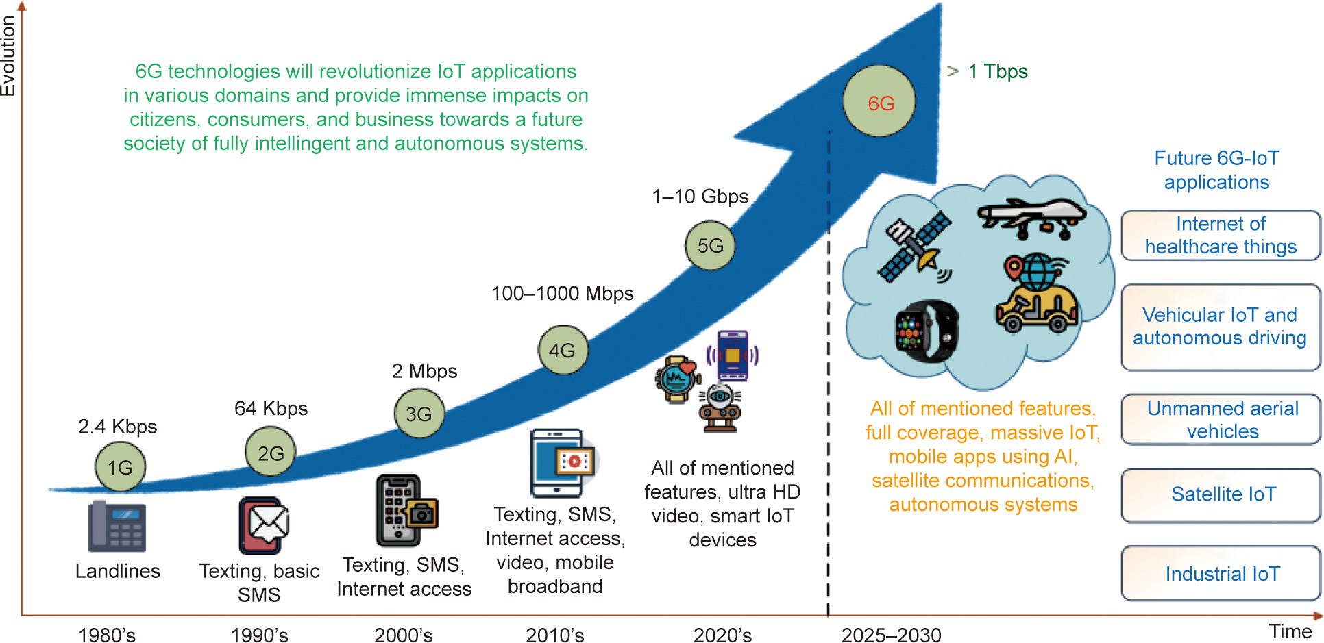
Fig. 1. The evolution of wireless networks toward future 6G wireless communications. Kbps: kilobits per second; Mbps: megabits per second; SMS: short message service; HD: high-definition; IoT: Internet of Things; AI: artificial intelligence. Reproduced from Ref. [3] with permission.
THz technology is not new; it has been a special subject area in astronomy for over 70 years, and THz imaging for security and medical applications has been a hot topic for the past 30 years. Significant progress has been made, which is well reflected by many books and research papers published in this area [5–8]. The latest surging interest in THz wireless communications can be seen as another wave (a huge one) in the development of THz technology. A considerable amount of effort in recent years has already gone into studying and developing THz communication systems. Many review papers can be found in the literature [7–21]. However, all these review papers focus on either THz imaging or THz wireless communications and do not treat them as interrelated or integrated THz technologies (although Ref. [21] touches on both as a short magazine article).
In this tutorial review paper, we examine both THz imaging and THz wireless communication technologies, highlight major achievements and state-of-the-art developments in these fields, and identify their similarities and differences in order to better understand and explore these technologies. Moreover, we discuss the integration of these two technologies, highlight their challenges, and suggest future directions. The remainder of this paper is organized as follows: Section 2 introduces the basics of THz technologies, with a focus on radiation characteristics and signal generation. Section 3 reviews THz imaging technology from its past to the present, including its main methods, achievements, and challenges. Section 4 discusses THz wireless communications, covering its design architectures, the state of the art, the main challenges, and possible solutions. Section 5 compares both technologies, discusses their possible integration, and presents conclusions and future perspectives.
《2. THz basics》
2. THz basics
The THz frequency band has been defined in a few different ways. The most widely accepted definition of the THz band is that it ranges from about 10 THz to 100 GHz (0.03–3.00 mm in wavelength) and lies between the microwave and infrared (IR) frequency bands. Unlike microwave and IR technologies, THz technologies are not well developed, and there is a lack of relevant components, devices, and systems available on the market with reasonable costs. Consequently, the THz frequency band can be viewed as a gap between the microwave and IR frequency bands in the electromagnetic spectrum (and is thus called the ‘‘THz gap”) that remains to be explored and advanced. Thus far, the THz band has not been allocated and is free to use—a situation that is expected to change soon [22].
Astronomists have studied THz waves from space in order to gain a better understanding of the universe; in this way, they discovered the absorption feature of the atmosphere, which is useful for weather forecasting and remote sensing [5,6]. Since the 1990s, the use of THz for security and medical imaging has become a hot topic and significant progress has been made [7,8]. In this section, we focus on two special features of THz—namely, its radiation characteristics and signal generation/detection—which differ significantly from its radio frequency (RF) and microwave counterparts.
《2.1. Propagation characteristics of THz》
2.1. Propagation characteristics of THz
Like RF and microwaves, THz waves are nonionizing, nondestructive, and intrinsically safe for humans. However, their wavelength is shorter (1 THz is 0.3 mm = 300.0 μm in wavelength), so they provide finer resolution than microwaves for imaging. Although their penetration depth into most materials is not as good as that of microwaves, it is better than those of IR and visible light and can reveal concealed objects on bodies and in packages—which is the main reason why THz has been employed to produce fine images for medical and security applications. Radio propagation path-loss (Lp) is a major parameter for wireless communications and imaging and is governed by Friis’ formula [23]:
where Pt is transmitter power, Pr is receiver power,  is frequency, and r is distance.
Thus, the path-loss is proportional to the frequency squared and the distance r squared: The higher the frequency, the larger the path-loss. At a distance of 1 m away from the source, the path-loss is 32.4 dB at 1 GHz but 92.4 dB at 1 THz in free space— an increase of 60 dB. Furthermore, THz waves suffer from atmospheric frequency-selective absorption (mostly due to H2O and O2), as shown in Fig. 2 [1], and differ significantly in this way from RF/microwaves. The two curves in Fig. 2 [1] represent the standard sea-level attenuation and dry air attenuation. The low-loss windows indicated in the figure could be considered for relevant applications. It is obvious that THz attenuation is very high and sensitive to weather conditions; thus, it is not suitable for long-distance transmission. Some frequencies have very high absorption (e.g., 120, 183, 325, 380, 450, 550, and 760 GHz) and should be avoided for transmission applications. Band window 1 (between 200– 300 GHz) has attracted a great deal of research activity due to its low-loss feature.
《Fig. 2》

Fig. 2. Average atmospheric absorption attenuation as a function of frequency up to 1 THz. The two curves show standard sea-level attenuation and dry air attenuation [1]. W1: window 1.
Another important feature of THz is that scattering due to the dust around the THz band is more significant than that around other frequency bands because of the shorter wavelength [18]. As a result, THz wave propagation is very different from that of RF/microwaves. High path-loss is a major problem in THz communications. Current solutions involve increasing the transmitting power (although this is limited by current technologies), employing directional antennas with high gains, or using beamforming technologies. The dominant path is line of sight. Although reflection and diffraction also play important roles, they are less significant for THz than for RF and microwaves for wireless communications. The free space path-loss model in Eq. (1) is not suitable for multipath environments, and more complex and accurate models have been developed. Based on various models [18,24,25], a combined general formula is given below:

where n is the path-loss exponent, which is typically between 1 and 4 (1.7 for an indoor environment, as reported in Ref. [24]). σ is a zero-mean Gaussian random variable that represents the fluctuation caused by shadow fading. α is the attenuation factor due to atmospheric absorption, scattering, and diffraction, which plays a major part in THz propagation characteristics, as indicated in Fig. 2 [1]. For indoor environments, the partition loss could be very significant in THz [18].
《2.2. THz signal generation and detection》
2.2. THz signal generation and detection
The conventional electronic transmitters/sources and receivers/ detectors used for RF/microwaves are powerful, compact, affordable, and suitable for room temperature; however, the development of equivalent devices still presents a major problem for the THz band. The current slow progress on THz research and development is mainly due to a lack of THz hardware—especially compact and affordable THz sources [8]. There are essentially two ways to generate a THz wave: One is to use an electronic source to double or triple the frequency to the desired THz frequency; the other is to use an optical source or sources to down-convert the signal to the desired THz frequency. Neither are very efficient, and the THz signal generated is usually small (less than 10 mW), which limits its applications. Previously, the most popular THz sources were time-domain-based broadband systems using a femtosecond laser and a photoconductive antenna to generate THz radiation. The main drawbacks of such systems include high cost and relatively low power; thus, further efforts have been made to develop new THz sources, and good progress has recently been achieved. For example, the quantum cascade laser (QCL) is now available. This was the first semiconductor source that could radiate reasonable power in THz. However, this THz source has not yet reached the full commercialization stage because it still requires cryogenic cooling, which seriously restricts its use in practical applications. The utility of this source would increase dramatically if it could function at room temperature.
Fig. 3 [26] provides a good overall view of the output powers of different THz sources. On the low-frequency side, electronic devices such as impact ionization avalanche transit-time (IMPATT) and Gunn diodes can generate relatively high power of over 1000 and 100 mW, respectively, at frequencies up to about 100 GHz. As the frequency increases, the output power decreases significantly. Resonant tunnel diode (RTD) oscillators can operate at higher sub-THz frequencies but with relatively low power levels (< 1 mW). On the high-frequency side (from an optical device), the QCL is the most promising power-generating source, although current devices mainly operate through a laser mixer or femtosecond laser pulse sources. An alternative THz-generation approach is based on intracavity difference-frequency generation (DFG) in a dual-wavelength mid-infrared (MIR) QCL [26]. These devices, which are known as THz DFG-QCLs, use a QCL active region engineered to exhibit a giant inter-sub-band nonlinear susceptibility for an efficient THz DFG process. Unlike conventional THz QCLs, DFG-QCLs are currently the only electrically pumped, monolithic, mass-producible semiconductor sources operable at room temperature (with a peak power of about 1.9 mW for 1–6 THz) [22]. Their drawbacks are that they require low temperature and a strong magnetic field.
《Fig. 3》

Fig. 3. THz output powers of different sources versus frequency [26]. IMPATT: impact ionization avalanche transit-time; RTD: resonant tunnel diode; NIR: nearinfrared; MIR: mid-infrared; LD: light-emitter diode.
In addition to the solid-state electronic THz sources mentioned above, significant progress has been made in the development of vacuum electronic device (VED) THz sources [27]. In a classic model, all sources of coherent electromagnetic radiation convert the kinetic energy of an electron current into electromagnetic field energy, as a principle. The electron transport medium in solid-state electronic THz sources is a semiconductor, while in VED THz sources, the electron transport medium is a vacuum. Electrons moving in a vacuum encounter no scattering. Consequently, VEDs are intrinsically superior at providing high THz power or high THz power density [28]. THz VEDs can offer over 12 orders of magnitude in power and over two orders of magnitude in frequency. In terms of power-frequency characteristics, the possible choices can be roughly divided into the following three classes.
• Compact sources with high mobility, including the backward-wave oscillator (BWO) [29] and the travelingwave tube (TWT) [30]. These are currently used for 0.1–1.0 THz with a power level of 1 mW–1 kW (continuous wave (CW) and pulsed).
• Compact gyrotrons with moderate mobility. These currently fill a performance window of 0.1–1.0 THz and 1 mW–1 MW (CW and pulsed).
• Stationary accelerator-based sources. These include freeelectron lasers (FELs) and beamline sources [31]. They are currently employed for the window of 0.2–10.0 THz (and beyond) and 10–109 W (average and pulsed).
VED THz sources are attractive, since they can provide high THz power. However, compared with solid-state semiconductor THz sources, they are usually larger and more expensive. Further development of materials and microfabrication techniques is especially important to enable further development of the most compact and powerful VED THz sources.
THz detectors—also known as THz receivers or THz sensors— can be divided into different categories according to the physical mechanism of detection. The first category comprises THz thermal detectors, which absorb THz photons and produce a physical change in the detector property as a result. For example, in a Golay cell [32], the absorption of THz photons by a membrane leads to its deformation, which then reads out, giving a measure of the input signal. Another category includes pyroelectric detectors, which consist of pyroelectric polyvinylidene fluoride (PVDF) foil coated on both sides with a thin layer of metal oxide. When the temperature changes due to THz radiation, the detector structure catches the charge generated by the pyroelectric effect of the foil and produces an electrical potential between the coatings. The spectra response of a pyroelectric detector is very broadband, reaching up to several THz; thus, these detectors are suitable for timedomain system (TDS) power measurement [33]. Another category of THz detector comprises semiconductor devices. The Schottky barrier diode (SBD) is widely used even under zero bias conditions. It can operate at ambient temperature and has an extremely fast response time [34]. The ability to integrate with other signalprocessing circuits using silicon or III–V semiconductor technology makes it attractive for low-cost and high-yield applications [35,36]. Field-effect transistor (FET) exhibits a high noiseequivalent power (NEP) that can reach as low as 10 pW·(Hz–0.5 ) for narrowband detection and to tens of pW·(Hz–0.5 ) for broadband detection [37–39]. GaN/AlGaN high-electron-mobility transistors (HEMTs) are employed for their high robustness against electrostatic shock [40]. Broadband detection from 0.2 to 1.2 THz is reported in Ref. [41]. Commercially available gallium arsenide (GaAs) FETs can significantly lower the cost while maintaining adequate responsitivity and NEP [42]. Practical THz detectors deployed in THz imaging systems are discussed in Section 3.2.
《3. THz imaging》
3. THz imaging
The first THz image was reported by Hartwick et al. [43] using an optically pumped molecular THz laser. The demonstration of optoelectronic THz imaging technology using femtosecond laserbased sources in 1995 by Hu and Nuss [44] generated a wave of research interest and activities in the field of THz science and technology. In the last two decades, tremendous advances have been made in THz imaging science and technology, in terms of both fundamental research and practical applications. In general, THz imaging techniques can be categorized into either optoelectronic or all-electronic imaging approaches, as shown in Fig. 4. The optoelectronic THz imaging approach is based on the optoelectronic generation and detection of THz radiation from pulsed or CW lasers using photoconductive antennas or nonlinear crystal, and it can be further divided into pulsed and CW THz imaging. In the all-electronic THz imaging approach, both THz generation and detection are purely electronic. This approach can also be further divided into passive and active THz imaging. In-depth descriptions of these THz imaging technologies and systems have been provided in numerous studies and reviews [45–48]. In this section, we focus on recent developments in these technologies.
《Fig. 4》

Fig. 4. Classification of THz imaging technology.
《3.1. Optoelectronic THz imaging technology》
3.1. Optoelectronic THz imaging technology
Imaging systems can be realized with both pulse-based and CW signals. In general, pulse-based systems measure single-cycle pulses in the time domain (broadband signals) and can obtain the information of a sample under testing over a large bandwidth at once, which is similar to a pulsed radar system. However, additional computation (i.e., fast Fourier transformation) is required in order to recover the information from the measured data. The signal-to-noise (SNR) ratio of the system can be an issue, particularly at higher frequencies, due to the large bandwidth used. In contrast, a CW system can provide an operating bandwidth comparable to that provided by photonic generation techniques, while maintaining a high SNR and fast acquisition time [49]. In addition, its fine spectral resolution and accurate phase measurement capability make the CW system attractive for fast imaging [50]. Since the most popular and advanced optoelectronic THz imaging system is the pulsed TDS, it is therefore the main focus of this section. A brief introduction of the CW THz imaging system is also provided at the end of this section.
3.1.1. The pulsed time-domain imaging system
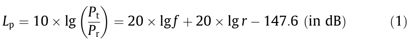
The core technology behind the pulsed THz TDS is the coherent generation and detection of short pulses using a femtosecond laser. As shown in Fig. 5(a), a beam splitter (BS) is used to split the nearinfrared (NIR) light from a femtosecond pulsed laser into two parts: a pump beam and a probe beam. The pump beam is focused onto the surface of a biased photoconductive antenna for THz generation. Under an applied electric field, the carriers that are photo-generated in a GaAs crystal by the femtosecond laser pulse produce a transient current, which results in pulsed waves at THz frequencies. The radiated THz pulse is collected, collimated, and then focused onto a sample under testing. The reflected THz pulse is then received and focused onto an unbiased photoconductive antenna for laser-gated THz detection [51,52]. Usually, a silicon lens (SL) is attached to the THz emitter/receiver antenna to enhance the THz radiation coupling efficiency. The timeresolved electric field of the THz pulse is received by scanning the NIR probe and a variable delay stage, as shown in Fig. 5.
One of the most distinctive features of the coherent detection scheme is that it allows the transient electric field—rather than the intensity of the THz radiation—to be directly measured as a function of time delay. Such a coherent detection scheme provides a range of image contrast mechanisms for which many novel applications have been demonstrated. Fig. 5(b) shows an example of a THz time-domain waveform, where the first peak is the THz reflection at the sample surface and the second peak is the THz reflection at the coating/core interface. THz images of different physical and structural properties can be constructed from the measured THz waveform.
《Fig. 5》
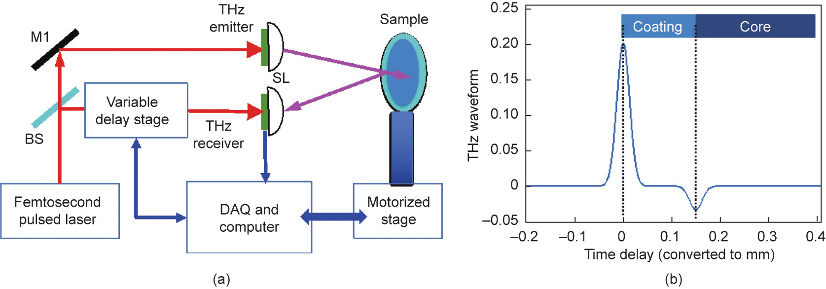
Fig. 5. (a) Schematic diagram of a typical pulsed THz imaging system, which is based on the coherent generation and detection of broadband THz pulses. (b) THz waveform simulated for a layered sample. M1: mirror; BS: beam splitter; SL: silicon lens; DAQ: data-acquisition.
A THz image can be obtained, usually in a pixel-by-pixel fashion, by moving the sample around the THz beam focus position using a motorized stage. For example, Fig. 6 [53] shows THz images of a chocolate bean that are obtained from about 4000 point measurements. At each pixel, the THz radiation reflected from the sample is recorded as a function of time. A full THz imaging measurement will thus provide a three-dimensional (3D) data cube in which the two axes describe the vertical and horizontal spatial dimensions, and the third axis represents the time-delay (depth) dimension. The recorded data cube can be analyzed to generate THz images. These coating-thickness maps display the uniformity of the coating layer over the tablet and can be used to identify problems in the tablet coating [54,55]. This time-of-flight measurement principle has also been applied for the nondestructive and quantitative characterization of automobile paints [56,57] and marine protective coatings [58].
《Fig. 6》

Fig. 6. (a–c) THz images of each layer of a three-layered chocolate bean. (d, e) THz map and photograph of a cross-section, respectively (solid arrows are guides to the eye). The color column presents the layer thickness and the unit is micrometer. Reproduced from Ref. [53] with permission.
3.1.2. Medical and biological applications
THz radiation has a low photon energy (i.e., nonionizing radiation) and does not pose any safety risk to human bodies. However, it is strongly attenuated by water; thus, it is very sensitive to water content. Consequently, there has been increasing interest in THz spectroscopy and imaging for biological and medical applications in the past decade [59]. Both ex vivo and in vivo THz imaging of human skin cancer have been reported, and a clear difference between cancerous tissue and normal tissue has been observed [60–62]. In addition, THz spectroscopy and imaging may be able to detect breast, tongue, liver, and colon tumors [63–68], without the need for any labels such as dyes. The underlying contrast mechanisms of this label-free THz imaging method are thought to involve the fact that cancerous tissue has a higher water content and cell density than normal tissue, resulting in THz spectral differences (e.g., refractive index and absorption coefficient) that can be used for cancer diagnosis.
Fig. 7 [68] shows an example of a THz spectroscopic image of rat fresh brain tissue, where the THz image was constructed using a principal component analysis of the measured THz spectra. The imaging data is able to correctly identify the tumor region because of the higher water content and cell density in that region. The presence of cancer often causes increased blood supply to the affected tissues, and a local increase in tissue water content results in an increased absorption coefficient.
《Fig. 7》
Fig. 7. (a) THz image and (b) hematoxylin-eosin stained image of fresh rat brain tissue [68]. The total number of measurement points in the THz image is 421 and the pixel size is 500 μm. The color of each pixel corresponds to the probability of a tumor calculated from the complex refractive index of the region, where a pixel value of ‘‘1” indicates 100% probability of cancerous issue and a pixel value of 0 indicates 0% probability of cancerous tissue (i.e., normal tissue).
Although X-ray and computer tomography (CT) provide better image quality and higher resolution, THz imaging outweighs traditional medical imaging technologies in two aspects. First, THz imaging provides not only amplitude but also spectral information; thus, it can give supplemental information, such as the type of human tissue [69]. Second, compared with CT and X-ray, THz imaging technology is intrinsically safe, which allows an increase in popular deployment, such as an intra-operational THz imaging probe to aid surgery procedures and in situ decision-making. In addition, Raman spectroscopy can detect the molecular and/or biochemical changes associated with specific chemical bonds and has been investigated for the clinical diagnosis of early-stage cutaneous melanoma [70].
One of the attractive features of THz imaging for biomedical applications is its penetration capability, which enables cancerous regions beneath the skin to be directly imaged. However, the absorption coefficient of tissue has been determined to be 12.7 mm–1 at 0.5 THz [63], which sets a fundamental limit on the effective detection depth of in vivo THz imaging under practical conditions. As the absorption coefficient of human tissue increases with frequency, THz radiation at lower frequencies will have better penetration capability. However, the spatial resolution of THz images will be poorer at lower frequencies, which may compromise the early detection of small tumors. Advances in near-field THz imaging, in which a spatial resolution beyond the diffraction limit can be achieved [71–74], may provide a fascinating method to address this issue.
Measurement specificity is another critical aspect of biomedical imaging applications. THz imaging technology has been demonstrated to be able to provide spectroscopic information of the tissue, thus providing the required measurement specificity [63,68]. However, these studies also indicate that cancerous and normal tissues have no sharp spectroscopic signatures in the THz frequency range. It has been found that the overall shape of the THz spectra of normal tissue, cancerous tissue, and water are all very similar in the frequency range up to 2 THz. This lack of sharp spectroscopic signatures presents a major challenge in reliably imaging and identifying cancerous tissues in real time within a clinical environment. Recent work in polarization-sensitive THz imaging and the on-chip dielectric probe may help to mitigate this measurement-specificity issue by providing additional information for characterizing tissue properties.
3.1.3. Future trend of THz time-domain imaging
THz time-domain imaging technology has demonstrated significant potential in a wide range of applications. Nevertheless, low spatial resolution is one of the main drawbacks of THz imaging. As the THz signal is recorded as a function of time at each pixel, THz images are obtained in a point-by-point fashion. For many practical industry applications, the image-acquisition speed of current THz time-domain imaging systems is prohibitively slow, which presents another problem.
There are several possible means of speeding up the THz imaging process. One method is based on asynchronous optical sampling, which offers extremely high data-acquisition (DAQ) rates that are orders of magnitude faster than those of conventional pulsed THz imaging systems [75]. Efficient THz generation is essential for such a high image-acquisition speed. Another method is to develop more efficient and powerful THz photoconductive emitters by incorporating nano-patterned metal contacts, as shown in Fig. 8 [76]. By using 3D plasmonic contact electrodes, the majority of photocarriers are generated in a sub-picosecond timescale to efficiently contribute to THz radiation. A record-high optical-to-terahertz power-conversion efficiency of 7.5% has been reported [77]; however, this value is still relatively low, and further improvement is possible.
《Fig. 8》

Fig. 8. A photoconductive antenna with nano-patterned contacts. The ‘‘fingers” of the structure reduce the photocarrier transport times to the contact electrodes and allow the plasmonic coupling of laser photons into the semiconductor, thereby improving the performance of the device. Vbias: bias voltage; Ebias: bias electric field; Epump, Hpump, and Kpump represents the direction of the electric field, the magnetic field, and the propagation of the pump wave, respectively; LT-GaAs: low-temperature-grown gallium arsenide; Au: gold. Reproduced from Ref. [76] with permission.
A more elegant way to significantly increase the imageacquisition speed is to use parallel detection. One innovative attempt to implement parallel detection involved the use of a large-area electro-optic crystal, where both the THz beam and the femtosecond optical probe beam were projected [78]. This technique was recently used to visualize the propagation of broadband pulsed THz radiation through an object [79]. This parallel detection scheme preserves all the benefits of THz time-domain imaging, such as time-of-flight and spectroscopic imaging. Its main drawback is that an amplified femtosecond laser system is usually necessary to drive the charge-coupled device (CCD) camera. Nevertheless, this work demonstrates the possibility and significance of video-rate THz imaging.
Another approach to speed up image acquisition utilizes the concept of compressed sensing [80–82]. A THz wavefront traveling from an object to a single-point detector is spatially modulated sequentially by a set of planar two-dimensional (2D) masks. This approach results in a significant improvement in imageacquisition speed compared with the traditional raster scanning method. It has also been reported that THz spectroscopic imaging is possible using a single-point detector based on compressed sensing, which allows both structural and chemical maps of a sample to be obtained [83]. To realize high-speed imaging using compressed sensing, a high-speed and multi-pixel THz spatial light modulator that can be controlled electronically is needed. Advances in active metamaterial-based THz spatial light modulators may enable the further development of compressed THz imaging for real-world practical applications [84].
3.1.4. The CW THz imaging system
The pulsed THz imaging systems discussed above have many attractive advantages, but they require expensive femtosecond laser systems and have problems producing fine spectral data. Thus, researchers are interested in developing less expensive alternatives with higher spectral resolution, without giving up the advantages of a coherent detection scheme. All-optoelectronic CW THz imaging systems, which utilize CW lasers, have been shown to be good alternatives to pulsed THz imaging systems [59]. The first implementation of an optoelectronic CW THz measurement system was demonstrated by Verghese et al. [85], who employed the optical beat signal from two CW Ti:sapphire lasers operating at different wavelengths (the difference was in THz) to generate and detect a THz signal using photoconductive antennas. A CW THz system based on compact and inexpensive semiconductive lasers has also been demonstrated [86], and the power radiated by THz antennas on low-temperature-grown gallium arsenide (LT-GaAs) has been improved by optimizing the antenna design and the LT-GaAs material properties [49,87]. Again, further improvement is still possible.
Fig. 9 shows a typical CW THz imaging system that is based on the photomixing of two CW lasers operating at different frequencies in a photoconductive emitter. As an example, the two tunable diode lasers are made to be collinear using an equal BS. The combined beams are focused onto the emitter and detector photomixers, respectively, which are made on LT-GaAs with an ultrashort carrier lifetime. Electron and hole pairs are generated in the photoconductive emitter when absorbing above-bandgap light. The modulation of the conductance of a photoconductive emitter at the frequency difference of two laser diodes results in CW THz radiation when a bias voltage is applied to the emitter. The resulting THz wave is radiated through a hyper-hemispherical SL as a collimated THz beam. A similar lens couples the THz beam to the detector via two focusing lenses. The DC homodyne output signal is detected by a lock-in amplifier referenced to the emitter bias modulation. The DC signal is maximized when the THz beam and optical beat arrive at the detector in phase (tuned by a timedelay stage); thus, it is possible to measure both the THz electric field amplitude and phase [85]. To cover a desired range of frequencies, the THz frequency can be tuned by means of mechanical adjustment.
《Fig. 9》

Fig. 9. Schematic diagram of a typical CW THz imaging system.
CW THz imaging systems have several advantages, such as higher compactness, higher imaging speed, higher spectral resolution, and lower cost, in comparison with pulsed THz imaging systems. They have been demonstrated to be promising for a wide range of applications [88] including biological applications [89] and gas sensing [90].
《3.2. All-electronic THz imaging technology》
3.2. All-electronic THz imaging technology
All-electronic THz imaging technology promises a more compact and faster system, which is necessary for many practical applications. This technology can be divided into passive or active imaging systems. Active imaging requires both a THz source and a THz detector, while passive imaging does not require a THz source. A passive imaging system operates by receiving the THz radiation that is naturally released from the object combined with reflections from other blackbody radiation sources in the environment. One of the driving forces to develop all-electronic THz imaging technology is its potential for security screening applications, since THz radiation is safe for people and can penetrate fabrics and other materials for the non-contact detection of concealed dangerous objects [91,92].
Passive THz imaging has been demonstrated to be a versatile imaging technique for real-time concealed object detection and recognition [93,94], and many commercial security imagers are passive systems, partly due to the relatively simple architecture. Fig. 10 shows a schematic diagram of a passive THz imaging system. It has four main units: ① imaging optics to form an image of the object at the detector plane; ② scanning mechanics and its controller; ③ a THz receiver unit, including a THz antenna, detector, spectrum analyzer, and amplifier; and ④ a DAQ card and a computer-based image reconstruction, processing, and display unit.
《Fig. 10》

Fig. 10. Block diagram of a passive THz imaging system.
For security screening applications, passive THz imaging detects the natural blackbody radiation either emitted directly from a human object or scattered from the object by a uniform blackbody source such as the sky. The weak human radiation at THz frequencies requires very sensitive THz detectors or detection schemes. Superconducting detectors have an established position in THz radiation detection systems. Superconducting antenna-coupled microbolometers provide an excellent SNR, making them attractive for passive THz imaging. THz images have been obtained in the frequency range of 0.2–1.0 THz at a near video rate by using a 64- pixel linear array of superconducting microbolometers, aiming for the standoff detection of concealed weapons in real time [94]. More recently, Hassel et al. [95] reported a passive imaging system based on a kilo-pixel kinetic inductance bolometer array operating at two bands (0.25 and 0.50 THz) for people-screening applications. These superconducting detector-based passive THz imaging systems require cryogenic-temperature operation; however, for many applications, such as security screening, room-temperature operation would be highly desirable.
For room-temperature operation, the GaAs Schottky diode is one of the most useful THz devices. As a low-parasitic device that operates well into the THz range, the Schottky diode provides useful detection and power generation for a number of practical applications including both THz imaging and THz communications. Mixers and multipliers, working as high as about 3 THz, have already been demonstrated [96]. A heterodyne detection scheme based on a GaAs Schottky mixer combined with a local oscillator has been used for passive THz imaging, and images of reasonable quality have been obtained at both microwave and THz frequencies [91,97,98].
In passive imaging systems, the challenge is to achieve detectors with sufficiently high sensitivity to efficiently capture THz signals, since human blackbody thermal radiation is extremely weak at THz frequencies. The background separation and temperature contrast in indoor environments are additional obstacles to passive imaging. In contrast, active THz imaging uses active THz sources to illuminate the object of interest; thus, the THz signal from an object will be orders of magnitude larger than its own blackbody radiation, making it easier to separate the object from its surrounding environment. Therefore, the active imaging approach not only yields the highest sensitivity but also provides more information about the identity of the object under screening.
Active imaging systems in the THz spectral region can be achieved with narrowband heterodyne receivers using a single THz detector; such an approach can achieve very high SNRs and large dynamic ranges, even with modest illumination power, although the image-acquisition speed is limited due to the necessary mechanical scanning [97]. In the past decade, significant advances have been made in the development of more compact and powerful THz sources [26] and more sensitive THz detectors and detector arrays, as summarized in a recent review paper [8]. A number of detectors have been developed for THz imaging [99–101]. The development of THz detector arrays, together with powerful THz sources, is of particular significance, as it allows video-rate THz images of a sample to be readily captured without the need for any mechanical scanning [102].
For security screening applications, temperature-related passive imaging could provide image data when an active system might fail, because specular reflection dominates in active THz images. On the other hand, an active image can differentiate among the contrasts of threat, body, and background temperatures, enabling results in cases where passive imaging fails [97]. Thus, the combined use of both active and passive THz imaging is a straightforward solution to overcome the individual weaknesses of each and provide a robust security screening method [103–105].
In summary, over the last two decades, THz imaging has grown from a promising curiosity to a flourishing research discipline, with ever-increasing commercial applications and scientific impact. The ability of THz time-domain imaging technology to nondestructively distinguish and characterize multilayer samples based on time-of-flight measurements is the key to many of the most successful commercial applications of THz technology so far. Nevertheless, an all-electronic THz imaging system can be made to be very compact, making it highly flexible and attractive for many industrial applications. Both optoelectronic and all-electronic THz imaging systems are commercially available. Table 1 [53–59,65,67,68,75,78,88,90,91,93–97,99–102,106–114] summarizes the working principles, advantages, applications, and challenges of each type of THz imaging approach.
《Table 1 》
Table 1 THz imaging technologies and their working principles, applications, and challenges.


FMCW: frequency-modulated continuous-wave.
《4. THz wireless communications》
4. THz wireless communications
Nowadays, there are many wireless communication systems in operation. 4G/5G cellular mobile and wireless fidelity (WiFi) systems are two examples. A THz wireless communication system is just another wireless communication system, which has an operational frequency in the THz band. It is not meant to replace any existing wireless systems but to add new capabilities and applications to what is already available. This frequency change results in both benefits and challenges. The main expected benefits are the ultra-wide bandwidth and possible high-data-rate communications (over 1 Tbps). The envisaged applications are as follows [1–3]:
• Point-to-point data-intensive/ultra-high-speed communications for data-center, backhaul, and space communications, among other applications;
• Hotspot areas such as sports stadiums and airports;
• Holographic communications and virtual reality applications;
• Small-scale communications (e.g., nano or inter-chip communications);
• High-precision and high-resolution positioning and sensing;
• 6G wireless communication systems and beyond.
Among all these applications, holographic communications could be a key application for THz wireless communications, since holographic displays are considered to be the next evolution in multimedia experience, delivering 3D images from one or multiple sources to another or multiple destinations. The recent renaming of ‘‘Facebook” as ‘‘Meta” is a reflection of this trend. The essential system requirements for this type of communication are an ultra-high data rate, extremely low latency, and excellent synchronization. Security and data resilience are also vital for such an application [1].
As mentioned above, THz wireless systems are expected to be beneficial not only for traditional macroscale wireless networks but also for emerging paradigms such as wireless intra- and inter-chip communications and nano-communications. Recent developments in nanotechnology are likely to introduce a number of ground-breaking applications. THz wireless nanocommunication is particularly promising, mainly due to breakthroughs in novel materials such as graphene. For this reason, many research efforts are now targeting THz band nanocommunication and nano-networking, and it is anticipated that these trends will continue in the future. Refs. [19,115] provide a very good overview of current THz nano-communication and nano-networking research. More specifically, they discuss the applications that are envisioned to be supported by nanonetworks operating in the THz band, together with the requirements such applications pose for the underlying nanonetworks. These studies also provide an overview of current contributions to the different layers of the protocol stack, as well as the available channel models and experimentation tools [19]. As nano-communication systems are currently in their infancy, making them a reality is still fairly far in the future. Thus, this topic is not covered in this paper.
The frequency change from RF/microwaves to the THz band results in a shorter operational wavelength and a wide range of hardware and software issues, including smaller sizes and more complex propagation characteristics.
《4.1. THz wireless communication system architectures and realization》
4.1. THz wireless communication system architectures and realization
A wireless communication system should consist of at least a transmitter and a receiver, as shown in Fig. 11. A baseband processor may digitize the original information, which is then encoded, modulated, and up-converted through a typical heterodyne (frequency conversion) architecture to the desired frequency before being transmitted by an antenna. In the case of envelope detection, a single detection diode can be used. The availability and parameters of these devices will eventually determine the emergence and potential success of THz ultra-broadband wireless communications. There are many detection schemes; the direct detection scheme is currently very popular due to its simple and costeffective configuration, but it has lower sensitivity and requires the use of amplifiers to extend the transmission range. In contrast, heterodyne detection can improve the sensitivity of the receiver and uses vector modulation schemes to increase the transmitted data rate; moreover, the system performance can be further enhanced in the digital processing stage.
《Fig. 11》
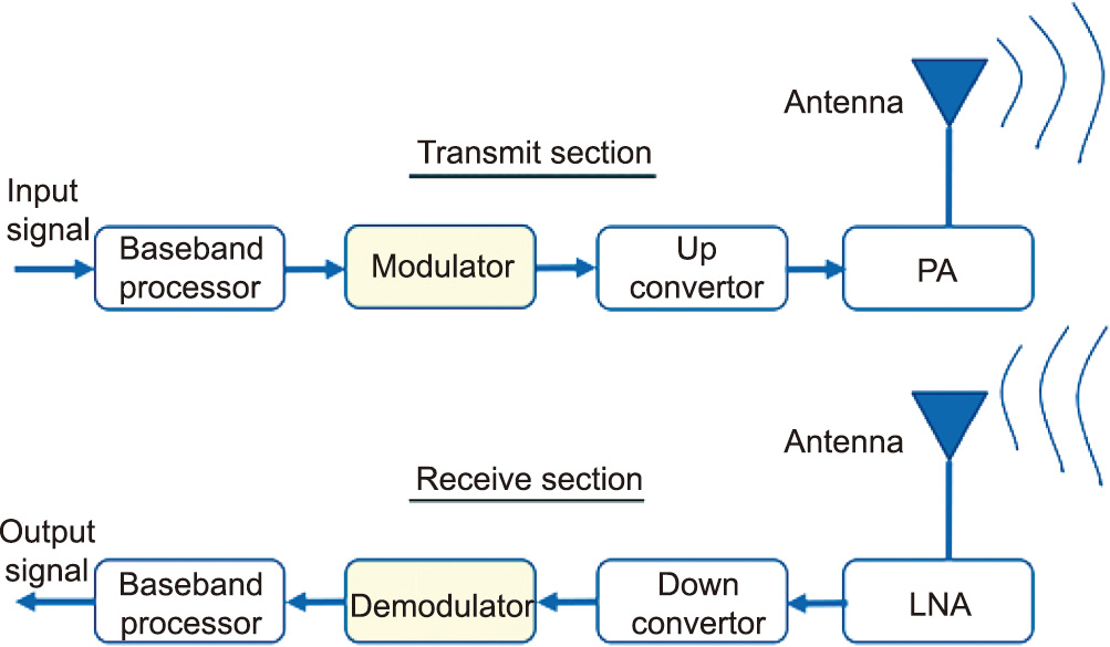
Fig. 11. A typical wireless communication system consisting of a transmitter and a receiver. PA: power amplifier; LNA: low noise amplifier.
Regarding RF front-end components, the operating frequencies and output powers of THz components cannot yet meet commercial requirements. One solution is to explore advanced semiconductor materials, such as silicon–germanium (SiGe) and indium phosphide (InP), and relevant technologies. In regard to baseband signal processing, THz systems must process Tbps transmission rates in real time, which is extremely challenging. A breakthrough is essential in advanced high-speed baseband signal-processing technology with low complexity and low power consumption. As for antennas, high gains are normally required to combat the high path-loss. These must be realized with a reasonable size and beam-steering functionalities. Moreover, THz propagation channel characterization and modeling are not well studied yet, and further research is required [18,116].
In practice, a THz transmitter can be created through three typical approaches. The first of these is the all-electronics-based approach, which consists of an RF signal generator, a data modulator, and a post-amplifier, if necessary. Usually, THz signals are produced by multiplying the output of a Gunn diode oscillator. The average output power of a few tens of microwatts is obtained in THz, which can be increased further by managing the saturated output power of the amplifier [12]. Other promising signal generators include integrated circuit (IC) oscillators made of semiconductor transistors, RTDs [96], Bloch oscillators [97], and plasmon oscillators [98].
The second approach is to use photonic techniques to generate and modulate THz signals: An optical signal whose intensity is modulated at THz frequencies is first generated using IR lasers, and then encoded by an electro–optic or electroabsorption modulator. Finally, the optical signal is converted into electrical signals by a photoconductor and then radiated to free space by an antenna. Semiconductor laser amplifiers are essential, since they are reliable and cost-effective [17]. A major issue in this approach is that the energy-conversion efficiency from optical to THz is very low; improving this efficiency is a very interesting topic.
The third approach is based on combined electro-optical systems, which may use THz lasers such as QCLs [117]. Direct modulation of the QCL is possible at modulation frequencies of over 10 GHz [118] in addition to the use of external THz modulators such as 2D electron gas (2DEG) semiconductor modulators and metamaterial-based modulators [12,119].
《4.2. Development of THz wireless communication systems》
4.2. Development of THz wireless communication systems
The idea of using THz for wireless communication has been around since the late 1990s. The first successful demonstration of THz communications was reported in 2004 [120], in which an audio signal was transmitted via a THz communication channel using a room-temperature semiconductor THz modulator, which was based on the reduction of a 2DEG. A standard THz TDS system was employed to transmit signals of up to 25 kHz over a 75 MHz train of broadband THz pulses.
Due to the large propagation loss, most THz communication systems use an operational frequency between 100–300 GHz, where the attenuation is at a local minimum in three valleys, as shown in Fig. 3 [26] and Refs. [1,18]. A very well-known example is the 120 GHz band system developed by Nippon Telegraph and Telephone Public Corporation (NTT) and Fuji Television Network Inc. and tested at the 2008 Olympic Games in Beijing [121]. This system first adopted a photonics-based transmitter in the wireless link with a bit rate of 10 Gbit·s–1 [122,123]. With progress in semiconductor IC technologies, an all-electronics-based transmitter was then introduced, which contributed to a reduction in size, weight, and cost, together with increased ease of operation [124,125]. Later, a power amplifier (PA) was employed to extend the transmission distance to 5 km, and a forward error-correction technique was successfully used to improve the long-term stability of the system [126].
The block diagram of this wireless communication system is shown in Fig. 12 [12], in which a THz source produces optical signals whose intensity is modulated at 125 GHz. An amplitude-shift keying (ASK) modulator is used to modulate the subcarrier for data transmission. The modulated subcarrier signal is amplified by an optical amplifier and input to a high-power photodiode, which converts the optical signals into RF signals and then amplifies and radiates them. The signal is received by an antenna and then amplified and demodulated by a simple envelope detection scheme. The RF receiver uses all-electronic devices and InPHEMT technology. A major advantage of such a photonics-based RF transmitter is that it makes the transmitter core (as shown in Fig. 12 [12]) very compact and lightweight; thus, it can be placed anywhere in the field. Furthermore, a photonics-based transmitter can be expanded to a multi-band system by using wavelength division multiplexing (WDM) technology; one of the three carrierfrequency bands with minimum atmospheric attenuation can be selected to ensure system performance in order to perform frequency hopping for better security. Such a system has achieved a maximum RF output power of 10 mW using a Cassegrain reflector antenna of 450 mm and a realized gain of 48.6 dBi (which is extremely high and not normally achievable in lower RF/microwave frequencies) [12,121].
《Fig. 12》
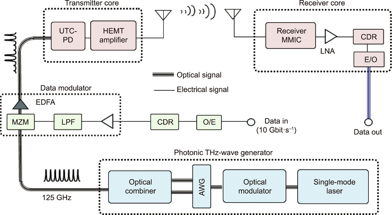
Fig. 12. Block diagram of the 120 GHz wireless link using a photonics-based transmitter. AWG: arrayed waveguide grating (for multiplexing); CDR: clock and data recovery; EDFA: erbium-doped fiber amplifier; E/O: electrical/optical (conversion); LPF: low pass filter; MMIC: monolithic microwave integrated circuit; MZM: Mach–Zehnder modulator; O/E: optical/electrical (conversion); UTC-PD: uni-traveling-carrier photodiode. Reproduced from Ref. [12] with permission.
Over the past decade, high-speed communication links between 100–300 GHz have developed rapidly, largely due to the progress made in the required hardware components. Modulators developed for optical-fiber communication systems have made high-data-rate complex modulation formats possible at these frequencies. At the receiver, SBDs can be employed for either direct or heterodyne detection. In the direct detection scheme, SBD detectors are used as square-law detectors for amplitudemodulated signals, as demonstrated using on–off keying (OOK) modulation at the W-band and over 100 GHz [127–130]. Realtime error-free data transmission was demonstrated for a 40 Gbps channel at 300 GHz and less than 1 m wireless transmissions by heterodyning two tunable optical light sources, as shown in Fig. 13 [131,132]. Polarization multiplexing was also used to double the data rate in a multiple-input multiple-output (MIMO) system, but it suffers from a significant cross-interference between the wireless channels. A better solid-state system has been developed recently [133] and will be discussed later in this section.
《Fig. 13》

Fig. 13. THz wireless link at 300 GHz using an SBD at the receiver [132].  : sub-carrier 1;
  : sub-carrier 2; Tx: transmitter; Rx: receiver.
Data rates of up to 100 Gbps were demonstrated at 237.5 GHz for a THz wireless system using a monolithic microwave integrated circuit (MMIC) receiver with quadrature phase-shift keying (QPSK) or 16-quadrature amplitude modulation (16-QAM) [134]. The transmission rate of 30 Gbps was achieved using 8-phase-shift keying (8-PSK) modulation at 240 GHz, and 46 Gbps was obtained at 400 GHz with OOK modulation by using a THz photomixer integrated with a broadband antenna. However, these systems suffer from phase noise on the generated THz waves, due to the uncorrelated phase noise of the two optical sources [135,136]
It should be pointed out that the THz wireless communication systems developed in recent years are mostly based on the photoelectric combination technique [16,17,130–132,134–137]. However, these systems employ many optical components based on various materials. Unlike electronics, in which the primary device is the transistor, there is no single dominant device in photonics-based systems. The range of devices required on a chip includes low-loss interconnect links, optical amplifiers and modulators, power splitters, filters, lasers, and detectors. These devices require a range of different materials and fabrication techniques, making it very difficult to realize all of them on a single chip. At the moment, these devices are not compatible with the integration and miniaturization of chips. Regardless of the endeavors put into implementing THz wireless communication systems by using solid-state electronic techniques, integrating THz systems into chips for future applications remains a major challenge [138].
Numerous efforts have been made in the past decade by different countries and institutions to develop all-solid-state THz communication systems, as reported in Refs. [17,126,133,139–149]. Here, we list some good examples. In 2009, the optical excitation devices of the THz communication system used in the Beijing Olympic Games were replaced by InP-HEMT MMICs [121]. The maximum data rate of this system was about 11.1 Gbps and it realized the error-free transmission of 10 Gbps signals over 800 m. In 2010, NTT Laboratory improved the THz communication system again. A structural diagram of the new two-way communication system achieved a 10 Gbps two-way data transmission rate and a 20 Gbps one-way data transmission rate [139]. In 2013, the Karlsruhe Institute of Technology (KIT) in Germany realized a single-input and single-output (SISO) wireless communication system at 237.5 GHz for a distance of over 20 m at a data rate of 100 Gbps (the highest at that time). This achievement resulted from combining THz photonics and electronics, whereby a narrowband THz carrier was photonically generated by mixing the comb lines of a mode-locked laser in a uni-traveling-carrier photodiode (UTC-PD). Its output was then radiated through a beam-focusing antenna. The signal was received by an MMIC comprising novel THz mixers and amplifiers [141].
More recently, a few Chinese universities and companies have developed all-electronic-based THz wireless communication systems, and good performances have been achieved. A schematic diagram of the 220 GHz transmitter and receiver developed by the University of Electronic Science and Technology of China (UESTC) is shown in Fig. 14 [17]. This THz communication system reached a real-time 3D high-definition (HD) video signal transmission of 3.52 Gbps over a communication distance of 200 m in the outdoor environment, with a bit error rate (BER) of 1.92 × 10⁻⁶ . A Cassegrain antenna with a gain of 50 dBi was employed to cover the expected distance.
《Fig. 14》

Fig. 14. Schematic diagram of the transmitter and receiver of a 220 GHz solid-state wireless communication system. PLL: phase-locked loop; BPF: band-pass filter; AGC: automatic-gain controller; SHM: subharmonic mixer; I/Q: in-phase/quadrature; LO: local oscillator; CO: crystal oscillator; I: in-phase; Q: quadrature. Reproduced from Ref. [17] with permission.
Very recently, a highly integrated solid-state THz MIMO wireless communication system was developed; its system architecture is presented in Fig. 15 [133]. A polarization-diversity technique was demonstrated to double the spectral efficiency in a line-of-sight environment. QPSK was employed as the modulation scheme, and the frequency was at 220–255 GHz. It should be noted that a pair of highly integrated single-chip transmitter and receiver front-end modules were developed using 0.13 μm SiGe heterojunction bipolar transistor (HBT) technology. It uses only a low-cost wire-bonded chip-on-board packaging solution for high-speed baseband signals. On the transmitter chip, each upconversion mixer is followed by a gain–bandwidth-limited four-stage PA for a communication distance of a few meters. Two independent in-phase and quadrature (IQ) data streams from the upconversion/downconversion paths on each chip are then directed to a common lens-coupled broadband on-chip slot antenna system. This way, two orthogonal circular polarizations, left-handed circular polarization (LHCP) and right-handed circular polarization (RHCP), can be transmitted with good isolation for quality communication, without the need for a high-speed depolarizer in the baseband for any relative orientation between transmitter and receiver modules. A slot antenna combined with a 9 mm-diameter SL provides a directivity of 23.5–27.0 dBi at 210–270 GHz for each of the modules, which allows the successful transmission of two independent QPSK data streams with an aggregate speed of 110 and 80 Gbps over 1 and 2 m, respectively, at 230 GHz [133].
《Fig. 15》

Fig. 15. Architecture of the transmittermodule of a wireless link with polarization diversity for left-handed circular polarization (LHCP) and right-handed circular polarization (RHCP) [133]. IQ-Tx: in-phase and quadrature transmitter; S2D: single to differential; freq mult: frequency multiplier; Ext ref: external reference.
A comparison of state-of-the-art electronic-based THz wireless links is given in Table 2 [142–145], while a comparison of recent photonics-based THz wireless links is presented in Table 3 [150– 159]. It can be seen that the best electronic-based THz wireless communication systems can achieve a data rate of 100 Gbps using 16-QAM and QPSK modulation schemes for a distance of about 2 m. The carrier frequency is typically less than 300 GHz, and the antenna gain is normally around 25 dBi. For a longer distance, a higher antenna gain and/or more output power is required. Compared with electronic-based systems, photonics-based THz wireless communication systems can use higher carrier frequencies and more channels to achieve higher data rates (> 600 Gbps).
《Table 2 》
Table 2 Comparison of state-of-the-art electronic-based THz wireless links.
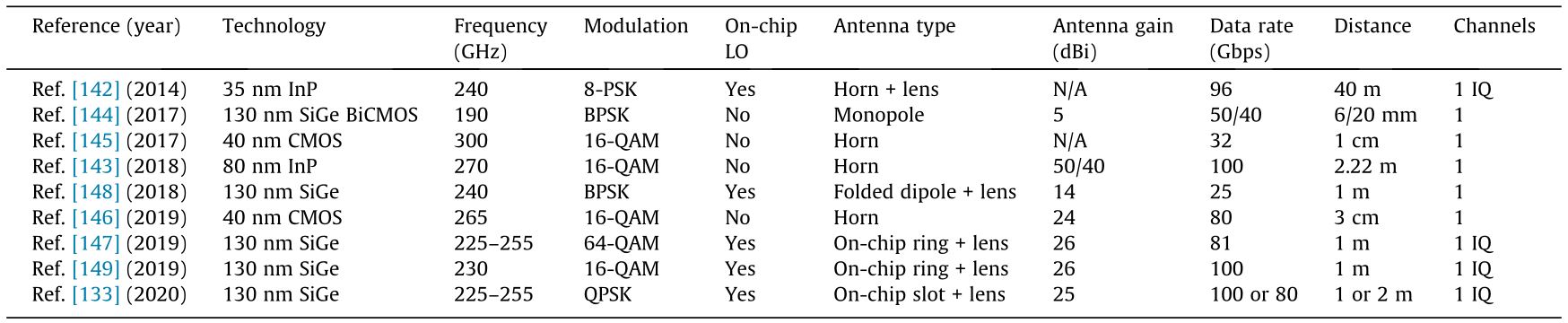
BiCMOS: bipolar complementary metal-oxide-semiconductor; CMOS: complementary metal-oxide-semiconductor; BPSK: binary phase-shift keying; N/A: not available.
《Table 3》
Table 3 Comparison of state-of-the-art photonics-based THz wireless links.

PDM: polarization division multiplexing; LUT: look-up-table; PS: probabilistic shaping; OFDM: orthogonal frequency division multiplexing; DFB: distributed feedback; NFDM: nonlinear frequency domain multiplexing.
《4.3. Main challenges for THz wireless communications》
4.3. Main challenges for THz wireless communications
It has become clear that recent advances in electronic and photonic THz transceiver design have enabled efficient signal generation, modulation, and radiation. Most of the reviewed THz wireless communication systems are below 300 GHz; in order to reach a data rate of greater than 1 Tbps, it is almost certain that the operating frequency will be above 300 to about 500 GHz. According to the International Technology Roadmap for Semiconductors (ITRS), the cut-off frequency of the silicon complementary metal-oxide-semiconductor (Si-CMOS) will exceed 500 GHz within a few years. In addition to a high data rate, the choice of higher carrier frequencies brings other important advantages. For example, the antenna size can be less than 1 mm, and the beam-forming antenna array will be a few millimeters in size. Such miniature antennas are integrable with communication terminals and equipment at a low cost. Considering the path-loss, 500 GHz is close to being an upper limit in ‘‘last-one-mile” outdoor applications, which differ from short-range indoor applications [18]. We believe that, in a few years, commercial THz wireless communication systems could be electronic-based, optics-based, or a combination of both electronic and optical devices; however, electronic-based systems will probably be the dominant mode eventually, due to the possibility of making a variety of highly integrated and costeffective systems [160]. The main challenges for THz wireless communication systems are in the following five areas.
4.3.1. Fabrication of electronic devices
While the fabrication of RF/microwave devices is mature, that of THz devices is not. Basic diodes and transistors do not yet work well in the THz band. High-precision mechanical processing has produced many high-quality mmWave and sub-THz antennas and waveguides but may struggle to meet the requirements for higher frequencies. Given the operating frequency of semiconductor devices up to the THz band, the effect of semiconductor materials and the distributed parameter effect of device packaging directly affect the circuit and system performance. In particular, the fabrication of THz amplitude modulators is very challenging, due to the small size. Modulation speed and modulation depth present even greater challenges. It is well known that natural materials cannot effectively and rapidly manipulate THz waves; thus, it is necessary to identify an appropriate material and structure to fulfill high-speed modulation of THz waves. Thus far, 2DEG composite materials (e.g., GaN HEMT) and 2D materials (e.g., graphene) have been applied in THz modulators. Thus, in the future, artificial materials with a response time of less than 1 picosecond in the THz band could be developed for device fabrication.
4.3.2. Power efficiency and heat dissipation
The power produced by current electronic-based THz systems is typically less than 10 mW; thus, the transmission distance is very short, unless a high-gain antenna is employed. As the power and operating frequency are expected to increase, power consumption and heat dissipation could become major problems, because the ohmic loss for conductive materials is proportional to frequency, and THz devices and systems are bound to be small in size. Power efficiency and heat dissipation have already become a problem for mmWave systems, including 5G mmWave mobile and base stations. Improving the power efficiency and dealing with heat dissipation could be major challenges for commercial THz wireless systems.
4.3.3. Speed of digital signal processing
Low complexity and efficient digital signal processing are required for THz communication systems to enable high-rate communication beyond 100 Gbps and even 1 Tbps within the next decades. The sampling rate of analog-to-digital converters (ADCs) scales up, corresponding to the larger bandwidths of THz communication. However, it is no longer feasible to build devices that meet the demands for size, weight, power, and bandwidth. For example, high speed (e.g., ≥ 10 G samples per second) and high precision (e.g., ≥ 6 bits) ADCs are either unavailable or may be too costly and power-hungry for devices. To address this problem, low-resolution ADCs are used to quantize the received signal. It has now become evident that efficient THz-band signal processing is crucial, for two reasons: First, it is necessary to take massive-MIMO antenna systems into account in order to overcome the problem of very short communication distances due to severe power limitations and propagation losses. Second, it is necessary to surmount the mismatch between the bandwidths of the THz channel and the digital baseband system, as doing so will effectively reduce the hardware cost and power consumption [161].
4.3.4. Design, simulation, and measurement tools
The computer-aided design of communication systems has become an industry-standard practice that significantly reduces development time and costs. However, current design and simulation tools are relatively accurate only for frequencies up to about 100 GHz, since many device models for higher frequencies are not accurate or not known. With the operating frequency of semiconductor devices in the THz band, the effect of semiconductor materials and the distributed parameter effect of device packaging become much more significant than at lower frequencies. The accuracy of the nonlinear model and the parameter extraction of semiconductor devices directly affect the circuit design and determine the system performance. Furthermore, mixers, amplifiers, and multipliers are highly precise nonlinear devices with complex properties. It is very challenging to improve the current design and simulation tools to support THz communication devices and system designs. Furthermore, as the operational nature toward THz becomes a multi-physical level (electronic, electromagnetic, thermal, etc.), multiphysics simulations may be inevitable in order to better simulate reality.
Other relevant research and development tools include measurement equipment and facilities, which are mostly available but expensive and with limited functions. There is a growing demand for affordable and accurate simulation and measurement tools.
4.3.5. THz wave propagation and 3D signal coverage
THz communication systems bring new and pressing challenges that have never been seen at lower frequencies. For example, the THz band suffers from very high spreading loss (> 94 dB for 1 m at 1 THz) and highly frequency-selective molecular absorption loss, as discussed in Section 2, which profoundly decreases the THz transmission distance [18]. Furthermore, the high reflection and scattering losses attenuate non-line-of-sight rays significantly, and the short wavelength makes THz signal propagation very vulnerable to blockages. Objects such as the user, moving humans, and inherent indoor constructions (e.g., walls and furniture) can act as impenetrable blockers. Thus, the propagation characteristics of the THz band are unique and differ from those of RF/microwaves. This motivates the research and development of new communication paradigms and novel signal processing and channel modeling tools to tackle these challenges. Ensuring 3D signal coverage for the desired applications is another major challenge for THz wireless communication systems.
《5. Discussion and conclusions》
5. Discussion and conclusions
In this article, we have introduced and reviewed THz imaging and THz wireless communication systems in detail and presented state-of-the-art system performance. Although these two systems seem to be very different, they are in fact closely linked. In this section, we compare the two systems and then discuss how they could be linked or integrated to accelerate the development of THz technologies.
《5.1. Comparison of THz imaging and wireless communication systems》
5.1. Comparison of THz imaging and wireless communication systems
Just like a THz imaging system, a THz wireless communication system consists of a signal emitter/generator (a transmitter) and a signal detector (a receiver). At present, femtosecond pulse sources, which use mode-locked lasers and photoconductive switches, are the most popular commercial systems for broadband THz signal generation. Such systems are mainly applied for highresolution 3D imaging based on time and depth resolution. They consume a considerable amount of power (e.g., a kilowatt or more) and are not very energy efficient. In addition, most short-pulse systems are not cheap and can be very large in size. However, most wireless communications and related applications require compact, low-power consumption sources and high spectral purity. Recent progress in photonic technologies for optical communication systems has made the generation of desired THz signals possible using compact and power-efficient coherent THz systems. The most promising photonic technique for THz signal generation is the heterodyning of two optical sources with different wavelengths that are mixed in a photodiode or photomixer. The THz signal frequency is the frequency difference of the two optical sources [88].
Many of the THz sources and detectors that have been developed for all-electronic THz imaging applications can also be used for THz wireless communication, and vice versa [162,163]. This makes it possible to combine THz imaging and THz communication into a single integrated THz system. High-power THz sources are extremely desirable for both THz imaging and THz wireless communication and have attracted much research interest in both research fields. For THz imaging, the focus is on developing THz detector arrays (e.g., video-rate THz cameras), while for THz wireless communications, THz transmitters and receivers that can be compatible with complementary metal-oxide-semiconductor (CMOS) technology might be advantageous. A more detailed comparison of THz imaging and wireless communication systems is given in Table 4, which covers most of the important elements of both systems.
《Table 4》
Table 4 Comparison of THz imaging and wireless communication systems.

DSP: digital signal processor; ASIC: application-specific integrated circuit.
《5.2. Integration of THz sensing and communication systems》
5.2. Integration of THz sensing and communication systems
The simplest form of THz imaging is detecting or sensing. Recently, the integration of sensing and communications (ISAC) has become a hot topic [164]. As a step beyond simply sharing the spectrum, the co-design of sensing and communication is clearly an efficient use of resources, since this would offer significant gains in terms of spectral, energy, space, and cost. Thus, ISAC is a paradigm change in which the previously competing sensing and communication operations can be jointly optimized via the shared use of a single hardware platform and a joint signalprocessing framework. The ISAC system will provide object and environment information by means of high-resolution sensing and localization, which will in turn benefit the communication performance, as it will help to refine channel estimation. These ideas have already been applied to some novel applications, including vehicular networks, indoor positioning, and covert communications [165,166]. In addition to academic research, industrial effort on ISAC is also well underway. It is reasonable to assume that ISAC is becoming an emerging technology for 5.5G, 6G, and the nextgeneration wireless local area network (WLAN) standards.
Despite its great attraction, joint design is not an easy task. There are numerous challenges in terms of establishing the system architecture, network, and hardware, and signal processing. For system and hardware deployment, finding joint blocks in sensing and communication can promote the possibility of ISAC. Typical direct-conversion transceiver architects in wireless communication systems and frequency-modulated continuous-wave (FMCW) radar systems are summarized in Ref. [167]. Both systems share many hardware components, such as voltage-controlled oscillators (VCOs), phase-locked loops (PLLs), low noise amplifiers (LNAs), and PAs. However, the shared components must satisfy requirements from both sides. For example, the VCO in a communication system should have a wide tuning range to address high-volume data, whereas the nonlinearity introduced by the nonlinear varactor will distort the chirp waveform in FMCW systems. Therefore, a wide tuning range and linear VCO are required for ISAC. As for signal waveforms and processing, there are several candidates depending on different valuing factors [168]. The current dominating waveform for existing 4G and 5G communication systems is orthogonal frequency division multiplexing (OFDM); for radar sensing, the typical waveform is based on the FMCW transmission of chirp signals. The chirp signal possesses an inherent low peak-to-average power ratio (PAPR), which is beneficial in a communication system, although it has the disadvantage of a limited capability for carrying a large amount of data.
《5.3. Conclusions》
5.3. Conclusions
In this paper, we conducted a comprehensive review of THz imaging systems and wireless communication systems. THz imaging appears to be becoming mature, while THz communication is still in its early stage but is gaining significant momentum. Both technologies present similar challenges, as they use the same THz frequency spectrum and have some common hardware components, and both can be realized using photonic-based, electronic-based, or combined approaches. The development of commercially viable high-power room-temperature THz sources remains the greatest challenge in this field. Although the general principles and design approaches for RF/microwave communication systems can be applied to THz communication systems, THz presents a range of special features and problems to be dealt with, including component and device fabrication, propagation channels, design and simulation tools, measurements, algorithms, and software developments. It is envisaged that electronic ICs will play a major role in THz systems, and ISAC could be an excellent way to integrate current THz imaging with THz wireless communication systems. We believe that affordable and high-performance THz imaging and THz wireless communications systems will become a reality in the near future.
《Compliance with ethics guidelines》
Compliance with ethics guidelines
Yi Huang, Yaochun Shen, and Jiayou Wang declare that they have no conflict of interest or financial conflicts to disclose.


 京公网安备 11010502051620号


