
《1 Introduction》
1 Introduction
Semiconductor lasers are solid-state lasers based on semiconductor gain media, whose optical gain is usually achieved by interband-stimulated light emission. They utilize the natural cleavage planes of semiconductor materials as cavity facets, which have the advantages of high efficiency, broad wavelength coverage, compact size, high radiation resistance, direct electrical-pumping, high yield, good reliability, and easy and high-speed modulation. However, semiconductor lasers have the drawbacks of asymmetric beam, large beam divergence angle, poor spectral purity, and high processing cost.
This paper focuses on overcoming the disadvantages of semiconductor lasers, including the bad beam quality, poor spectral purity, large beam divergence, and difficulty in achieving intracavity control. Herein, the research and development of optically pumped vertical-external-cavity surface-emitting lasers (OP-VECSELs), micro- and nanolasers, and topological insulator lasers are briefly reviewed; the development route of semiconductor lasers is summarized; and methods are introduced that achieve the integration of new physics, new concepts, and new technologies under a multidisciplinary background. Furthermore, some suggestions for reference on the development of the semiconductor laser industry in China are provided.
《2 Several new semiconductor lasers》
2 Several new semiconductor lasers
The combination of new physics, new concepts, and new technologies with semiconductor lasers has brought new ideas into their development. Through the fusion of optics, electromagnetics, microelectronics, topology, and quantum mechanics, many new lasers have been proposed. They either have large-scale integrated application prospects, excellent beam and spectral quality, higher and more stable output power, smaller size, and a beam profile that can exceeds the diffraction limit, or they can facilitate modulation and nonlinear transformation, or have exciting reduced power consumption. The development of these new lasers represents the advanced semiconductor laser technology, as well as reflects the development status of physical theory, engineering technology, and processing technology, which are worthy of deep research. Among these, OP-VECSELs, micro- and nano-lasers, and topological insulator lasers (Fig. 1) represent the new semiconductor lasers, resulting from the fusion of solid state lasers and semiconductor lasers; lasers and optics; and lasers and emerging physics, respectively. This article will discuss in more detail their rich physical connotation and application potential.
《Fig. 1》
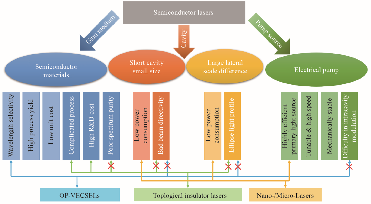
Fig. 1. New laser characteristics.
《2.1 Optically pumped vertical-cavity surface-emitting laser》
2.1 Optically pumped vertical-cavity surface-emitting laser
An OP-VECSEL, also known as an optically pumped semiconductor laser (OPSL), or semiconductor disk laser (SDL), is the combination of a semiconductor laser and solid-state laser. OP-VECSELs use semiconductor materials as the gain chip, similar to the vertical-cavity surface-emitting laser (VCSEL); the resonant cavity structure is solidstate-laser-like, usually comprising a distributed Bragg reflector (DBR) on the semiconductor chip and an external cavity mirror. Moreover, optical pumping is adopted, which can provide a more flexible working mode and better device performance. The semiconductor gain chip can provide a variety of wavelength selections and a wide spectrum tuning range. The solid-state laser cavity makes it easy to insert optical components inside the cavity to perform sum frequency/difference frequency, beam shaping, Q-switching, and mode-locking. Furthermore, an ultrashort pulse laser, a special wavelength laser, a terahertz laser, and a multi-wavelength laser, among others, can be produced via the laser intracavity control to meet a variety of special application needs.Due to the characteristics of OP-VECSELs, the main research content in this field is currently focused on output power improvement, wavelength tunability, ultrashort- or ultrahigh-intensity pulse generation, and specific wavelength or multiwavelength operation. In terms of wavelength coverage, VECSELs have now achieved full band coverage of light, i.e., from the ultraviolet to the terahertz band. Table 1 shows the typical parameters of VECSELs for different emitting wavelengths. The shortest lasing wavelength achieved through intracavity frequency doubling can reach 244 nm [1], while the longest wavelength achieved using dual-wavelength intracavity difference frequency can reach 1.9 THz [2]. At present, the highest single-chip output power of a VECSEL is recorded as 106 W [3], the highest repetition frequency is 175 GHz [4], and the minimum emitting pulse width is 60 fs [5].
《Table 1》
Table 1. Vertical-external-cavity surface-emitting laser (VECSEL) characteristics in different wavelengths.

VECSELs are suitable for emerging technologies, such as communication under special environments or through special media, and sensing with specific wavelengths, which require high-performance light sources. A significant number of existing technologies in the fields of solid-state lasers and semiconductor lasers have been used to improve the output performance of VECSELs. Moreover, solid-state laser technologies such as resonator design, spectral control, intracavity frequency doubling, mode-locking, multi-pass pumping, as well as semiconductor-related process technologies such as chip preparation and thermal management, have provided strong support for the development of VECSELs.
The high performance and flexibility of VECSELs make them suitable for customized applications (Fig. 2). Their development should focus on platform construction, and close tighten with the application. On one hand, it is necessary to conduct innovative research and development on the platform technology of the VECSEL, the general chip fabrication, universal thermal management, and general beam control, among others. On the other hand, there is an urgent need to develop and expand specific technologies for high-performance laser systems for specific applications, such as development for specific wavelengths, high beam quality, narrow linewidth, and wide tuning range.
《Fig. 2》
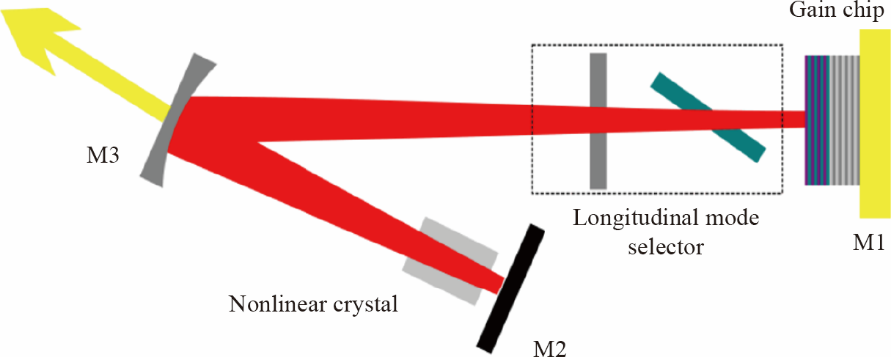
Fig. 2. Schematic of VECSEL.
《2.2 Micro-/nano-lasers》
2.2 Micro-/nano-lasers
Micro- and nano-lasers generally refer to lasers whose size or mode size is close to or less than the wavelength of the emitted light. Due to their characteristics of compact structure, low threshold, and low power consumption, these lasers have broad application prospects in the field of high-speed modulation. Furthermore, these characteristics are crucial for photonic integrated circuits, optical storage, and photonic computer applications. They can also be widely used in the field of biochips and laser medical treatment as well as other emerging fields such as wearable devices.
As a reduction in size often implies a reduction in the threshold current and power consumption, to improve the energy conversion efficiency, the volume of semiconductor lasers has been reduced by approximately 5 orders of magnitude in the past fifty years. The miniaturization of semiconductor lasers began with the VCSEL, whose size was reduced to the order of tens of micrometers; thus, they have been widely used in the fields of communication and consumer electronics. To further reduce the volume and obtain higher performance, various methods have been used to compress the cavity length, and new designs of the resonant cavity have been proposed. For example, the micro-disk laser uses whispering gallery modes, the surface plasmon polariton laser has a metal core-shell structure, and some new types of heterojunction lasers based on two-dimensional (2D) material and a Fabry–Perot cavity have been proposed. Table 2 briefly introduces the structure and characteristics of different types of micro- and nanolasers. With the establishment of emerging scientific technologies,such as quantum optics, surface plasmon polariton, and 2D materials, micro- and nano-lasers have achieved a breakthrough in the three-dimensional (3D)-size diffraction limit. Based on the surface plasmon, dielectric mode SPASER (plasmonic laser), the lateral scale can be reduced to below 260 nm [14] and electrically pumped. The 2D-material gain medium based on a transition metal dihalide for a miniaturized laser can provide a material gain, which is several orders of magnitude higher than that of traditional semiconductor quantum well materials, and break the 3D diffraction limit [15]. In addition, the introduction of quantum dots provides a new manner of improving the laser gain medium performance.
《Table 2》
Table 2. Difference in characteristics between several nano-/micro-lasers.
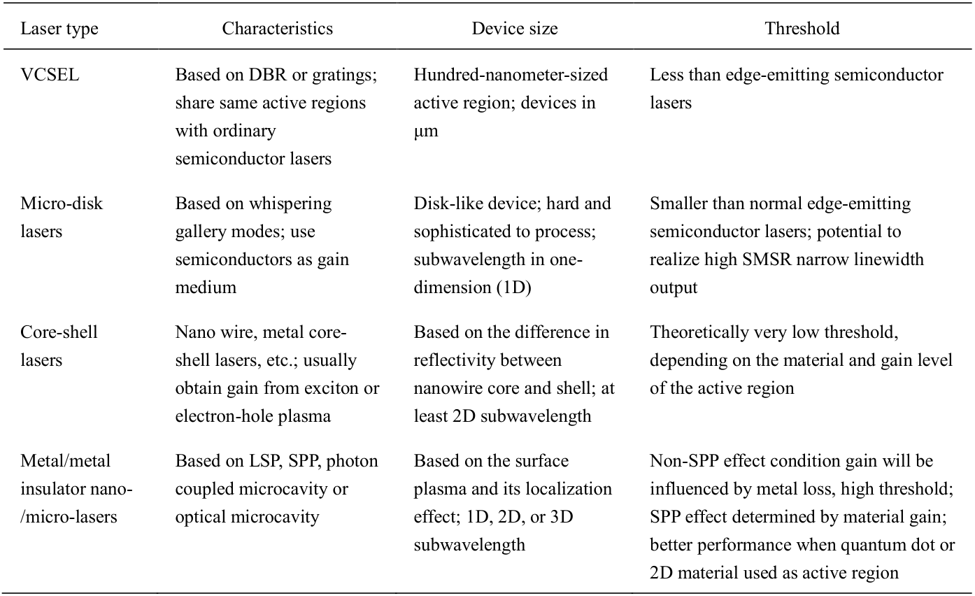
Most micro- and nano-lasers are concepts or remain in the research stage, excluding VCSELs, which have been successfully commercialized. However, the small size of micro-disk lasers; low threshold and high modulation rate of photonic crystal lasers; flexibility of the wavelength of nanowire lasers; and balanced performance of SPP lasers make them broad-development-prospects in their respective application fields.
The different applications of micro- and nano-lasers have different performance requirements, and the suitable technical solutions may vary significantly. For example, in the field of its largest target market, optical communications and optical information processing, solutions based on semiconductor processing and electrical pumping are more suitable for the requirements of productivity, reliability, and long lifetime. Conversely, in the field of biomedical technology, under the strict requirements of size and biocompatibility, optical pumping and selforganizing solutions will be more competitive.
The development of micro- and nano-lasers requires strong technical capabilities. In addition to the micro-nano processing technology, the material growth technology, device-manufacturing process, and even testing and packaging technology need to be specially developed.
《2.3 Topological insulator laser》
2.3 Topological insulator laser
A topological insulator laser is a combination of semiconductor laser technology and the concept of a “topological insulator” in condensed matter physics. Using the concept of edge states in topology, this laser is insensitive to disturbances and defects in the internal structure of the device, and easily realizes high output power, high robustness, and a stable mode. Particularly in high-power lasers and emerging nanophotonic lasers, the property of insensitivity to scattering loss and random manufacturing defects makes them suitable for applications in high-power modelocked laser arrays and quantum information generation/transmission.
First proposed in 2018 [16,17], the excellent output stability and insensitivity to structural defects of topological insulator lasers based on semiconductor topological structures have drawn considerable attention and become a popular research topic in related disciplines. Presently, most of these lasers utilize the semiconductor micro-nano topology as the structural unit and realize the resonance function through the optical field or electronic limitation formed by the topology, thereby realizing directional single-mode lasing. Table 3 shows different types of topological insulator lasers. As an example, the nanocavity topological laser established by Peking University in 2020 [18] is a single-mode laser that emits vertically, and output direction adjustment can be conducted via the device topology. These lasers have a high directivity, small volume, low threshold, narrow linewidth, and high sidemode suppression ratio for both horizontal and vertical modes. In addition, by combining the concept of topological symmetry and other new lasers, the symmetric honeycomb plasma-photon (diffraction) topological SPASER [19], hexagonal, plasmon metal-nano-shell core-array SPASER [20], and terahertz compact quantum-cascade topological laser [21] have been realized, among others.
《Table 3》
Table 3. Examples of several topological lasers.

The development of topological insulator lasers is still in the stage of proposing and verifying the physical concepts. The current focuses include cross-disciplinary strengthening, promoting multidisciplinary and multifield cooperation, combining the characteristics of semiconductor lasers, and innovative theoretical research and experimental verification.
《3 Current status of semiconductor laser industry》
3 Current status of semiconductor laser industry
The semiconductor laser industry has become the basis of the entire laser industry, which is an integral part of human society. According to a forecast, the global laser sales market is expected to maintain a 6% growth rate in 2019, reaching 14.6 billion USD. Among them, the market size of semiconductor lasers (including direct semiconductor lasers, as well as pump sources of solid-state lasers and fiber lasers), is approximately 6.88 billion USD, accounting for approximately 50% of the overall laser market [22].
The entire semiconductor laser industry mainly includes several application nodes that are tandem arranged, materials, chips, devices, modules, systems, etc. However, the upstream materials and chip industry; the midstream devices or the downstream modules and systems industry; and the semiconductor laser industry are technologically intensive and require huge capital investment.
After decades of development, international customers are gradually paying more attention to the overall cost and comprehensive performance. In addition, the selection of laser products is becoming increasingly stricter. Recently, due to these factors, new development trends have emerged.
Considering application potential, semiconductor lasers are expanding from industrial applications to consumer applications, and their market size may grow explosively with competition being further intensified. The adoption of Lumentum’s VCSEL as a light source for 3D sensing in iPhones in 2018 was a landmark event of this trend. Lummetum has driven and guided the market’s development through years of deep cultivation in the consumer electronics industry. By innovating applications, Lumentum obtains enormous profit and has an advantage in competition over other leading companies in the field, such as II-VI and Finisar, without significant technological advancement.
From the perspective of semiconductor laser companies, the competitive situation is similar to that of the microelectronics industry in the 1990s. Both experienced the competition route from free competition of small- and medium-sized enterprises to the domination and division of the market by the “Big Mac”-type companies created through mergers and reorganization. For example, the merger of Lumentum and Oclaro and the reorganization of IIVI and Finisar, which have already been dominant in the industry, will inevitably have a significant impact on the survival status of the small- and medium-sized enterprises in the industry.
In recent years, new semiconductor laser companies have also achieved tremendous development, including large integrated design and manufacture (IDM) companies, foundry companies, and fabless companies, among others. Although they are extremely popular and are mainstream in the silicon industry, they are new to the semiconductor laser industry.
IDM (vertical integration) companies are application system companies that contribute to the production of semiconductor lasers; semiconductor lasers are their core competitors, but not the end product. IDM companies include solid-state laser, fiber laser, and laser processing enterprises, such as IPG photonics and Coherent. Most of these companies have achieved a complete integration of materials, chips, devices, modules, and systems within the enterprise, through either mergers and acquisitions or self-development. IPG, the first company to achieve “vertical integration,” has established its absolute superiority in the field of fiber lasers. Although there is an excess production capacity, semiconductor lasers are not sold as products by IPG.
Meanwhile, foundry companies are mainly engaged in providing manufacturing process services, such as epitaxy or chip process. In case of epitaxy, the enterprises include IQE in the UK, IntelliEpi in the United States, Landmark in Taiwan Province, and Sumitomo Chemical in Japan. Among these, the market shares of the entire epitaxial wafer occupied by IQE have reached 60%, and the market share corresponding to the application of VCSELs has reached 80%. In terms of chip technology, Taiwan’s WIN semiconductors corporation, Advanced Wireless Semiconductor, and Global Communication Semiconductor account for 90% of the entire semiconductor foundry market. These companies provide the most cost-effective, mainstream, manufacturing process technology, with optimal process equipment for compact device layout and material structures. They can service good quality products in a timely manner.
The fabless companies only engage in semiconductor laser design, packaging, testing, etc., and entrust foundry with production. Most fabless enterprises are small- and medium-sized; however, sometimes large enterprises will outsource production in a similar manner, and even switch to fabless enterprises, thereby reducing the overall cost. For example, although Lumentum has its own vertical integration capability, its VCSELs are mainly produced by IQE and WIN; whereas, Avago has stripped off the chip process unit and sold its factory in Colorado to WIN, becoming the third-largest shareholder of the company, and entrusting WIN with production.
Generally, IDM semiconductor laser companies have the advantage of product performance, while the combination of foundry and fabless companies has the advantage of better cost control.
Comparing the semiconductor laser industry with the upstream/downstream industries, the industrial driving ability is strong and the first-mover effect is clear. The proportion of semiconductor lasers in systems is much greater than that of their price. Semiconductor lasers are the core competitors of system applications; however, they cost less than 1% of that of the entire system sometimes. System verification of device functions and reliability requires long-term, massive closed-loop optimization. In addition, the cost of trial and error is considerably high, forming a high “threshold.” Thus, the system company lacks the willingness to risk changing their supplier of semiconductor lasers. As the semiconductor laser industry has matured, the gap between the leader and chaser has further widened. This is the main problem faced by Chinese companies, particularly after the outbreak of the Sino–US trade war, this problem has been fully exposed.
In recent years, China has vigorously supported the key technology of the chip industry in a targeted manner, and has obtained a certain foundation in terms of talents and technical reserves. The impact of the first-mover effect has been alleviated to a certain extent, but it will take some time to realize the effect of the applied policy.
The development of the semiconductor industry in China is significantly unbalanced. In the downstream system industry, industry leaders, such as Huawei and ZTE, have emerged in the communications field. Midstream optical module companies also include advanced companies, such as Inno Light who are internationally competitive. However, in the upstream industry, for the laser chips, the research and development as well as production capacity of related companies in China are inadequate, and the status in the field of material epitaxy is even worse. Related companies are generally small- and medium-sized, and hence, find it difficult to compete with foreign products in terms of product strength. Although the government’s support is enthusiastic, there is insufficient understanding of the chip industry, serious homogeneity, a lack of patience and top-level design, and a good industrial chain has not yet been formed. The entire industry is in a vicious circle where promising products cannot gain access to the market, and market funds are reluctant to support technology development. Some successful system companies have recognized this problem and made efforts to integrate industries vertically, but often encounter many difficulties and progression is slow.
《4 Development demands of the semiconductor laser industry in China》
4 Development demands of the semiconductor laser industry in China
The primary requirement of the semiconductor laser industry in China is to ensure national strategic security. Semiconductor lasers are the core components of optical communications, laser sensing, laser processing, and laser pumping. They can also be directly used in military fields such as for light detection and ranging, laser ranging, laser weapons, missile guidance, and optoelectronic countermeasures.
In addition, building a complete, closed-loop industrial chain; forming positive feedback; and accelerating the maturity of upstream core chip technology through market applications and using mature chip technology to drive the implementation of new achievements and applications is the best path for the development of related industries in China.
Further, the semiconductor laser industry in China is still and will be in a catch-up phase for a long time; thus, it is vital for the industry to achieve leadership in certain fields. Concerning the current status, developing new devices for new applications and occupying the “first-mover advantage” are effective ways to progress and even surpass the foreign counterparts.
Based on the above considerations, the new laser industries, which remain in development and have a certain distance from the market, are undoubtedly important breakthroughs for solving these issues.
First, although technology accumulation remains important, the gap between China and foreign countries in terms of the research and development of new lasers is relatively small. Supported by policy in recent years, China has achieved long-term development in the field of interdisciplinary integration and emerging semiconductor lasers. Particularly in the field of micro- and nano- optics and lasers, Chinese researchers have participated in or hosted many of the world’s top research results through international cooperation. If these results can be transferred industrially, a solid foundation for the development of China’s new laser industry will be obtained. Second, the new laser involves basic science. In recent years, China has attached great importance to the construction of basic disciplines, providing a talent base and development potential for the advancement of new lasers. Finally, in the new laser industry, development also remains at the first stage worldwide. Through national funds and policy support, we can concentrate on resolving difficult tasks; further, the development of China’s new laser industry will have the ability to occupy the first-mover place in the world.
Nevertheless, the accumulation of technology and development of the industry cannot be achieved overnight; we must see both sides of the coin. Foreign companies possess the technical theory, talent reserve, process flow, and production equipment. The enterprises remain predominantly small- and medium-sized. In addition, the products are mainly aimed toward low- and mid-end markets, which cannot achieve the essential industrial transformation. Technology output is still based on a limited number of technologies or patents, and it cannot form a complete industrial chain, or establish a comprehensive system of industry–university–research integration. Moreover, the majority of manufacturing equipment continues to be imported; thus, foreign technical output is heavily relied upon, and true independent intellectual property rights cannot be achieved. Therefore, policy guidance in the relevant field is urgently needed.
《5 Suggestions》
5 Suggestions
The semiconductor laser industry is a basic industry related to the national economy and people’s livelihood. The development of the semiconductor laser industry is of great significance to China for competing in the modern information society. China should take advantage of its domestic market capacity; develop new applications; adhere to the principle of the independent development of new technologies; encourage new concepts and interdisciplinary development of new theories and realize the development of new semiconductor lasers. The developing field of the new semiconductor laser industry still has a vast territory internationally. Combined with China’s policy advantages, scientific and technological development level, and talent reserve, in the next 10–20 years, China should cultivate excellent enterprises for new semiconductor lasers that can compete with the world’s leading laser industry giants, so as to seize the strategic commanding point and provide the power source for further development of the semiconductor laser industry in China.
First, in view of the difficulties and challenges in the development of the semiconductor laser industry, China’s primary task in the near future is to selectively and pertinently support the development and production of semiconductor lasers of the high power, narrow linewidth, and special wavelengths suitable for certain applications, including relevant scientific research and technology transfer. Moreover, China should fully evaluate the domestic devices, face the development gap, and improve relevant technologies to ensure the safety of national equipment.
Second, in the civilian application field, it is important to promote the localization of cost-sensitive semiconductor lasers; make full use of market orientation and the company’s motivation that are supplemented with local policies for guidance and support; pay attention to the differentiation of related products; and avoid development in chaos. For example, compared with telecommunications applications, the lifecycle of semiconductor lasers and modules in data center applications is shorter (approximately 3 years compared to 20 years), maintenance is easier, and the industry entry barrier will be relatively lower. In laser material processing systems, semiconductor lasers account for a high proportion of the total cost; thus, low- and medium-power material-processing companies are more willing to replace their expensive imported semiconductor lasers. This is another breakthrough point for domestic devices. In this replacing process, we can further cultivate local enterprises and talents.
Furthermore, the potential of existing technologies for new applications should be fully explored. For some mature or near-mature semiconductor lasers, such as VECSELs, the markets are still not being fully exploited. Aiming at certain applications, development or secondary development should be carried out to promote horizontal expansion. Using the close connection of system and application vendors to purposely improve laser technology, the “first-mover advantage” could be obtained.
The medium- and long-term policies should aim at localization and the independent development of high-quality semiconductor lasers, which requires more participation, and even domination by the government at the national level. If necessary, policy support and special funds can be used to ensure healthy development:
(1) Make full use of China’s significant advantages on the application side, and encourage the establishment of IDM companies or company groups. To realize the feedback loop of development and application of relevant devices, the maturity of crucial materials and devices should be promoted, and multiple IDM companies with a stable cooperative relationship should be established.
(2) Make great efforts to encourage and guide the application of domestic devices. State investment or subsidies should be adopted to establish a complete localized application platform to test alternative devices, and the evaluation of domestic devices should be realized under application conditions. Furthermore, policy-oriented and financial subsidies should be established to encourage the application of domestic devices.
(3) Establish an all-in-one technology platform with foundry function and independent intellectual property rights that can realize technology development as well as meet the full laser preparation needs of fabless enterprises. Microand nano-lasers could be used as the criterion to certify the comprehensive ability due to their harsh technical requirements. In particular, it is necessary to overcome the shortcomings, pay attention to the key technologies and processes, and provide technical support for the development of new semiconductor lasers.
(4) Encourage new concepts and new devices, and plan ahead to obtain the first-mover advantage. Research should be conducted on new semiconductor lasers and their corresponding processes, including topological insulator lasers; cross-industry, and front- and back-end interflow should be encouraged, and a shift should be made from new concept development to application-oriented technology development at an appropriate stage.


 京公网安备 11010502051620号


