
《1. Introduction》
1. Introduction
The photovoltaic (PV) industry is in a phase of rapid growth, annually increasing by 44% for PV installations from 2000 to 2013 [1]. China’s mainland and the Taiwan region entered the mass production market in 2004 and ramped up a PV industry with strong growth rates. By the end of 2013, their market share was approximately 70% of worldwide shipments [1]; however, their total cumulated installations in 2013 were occupied by only 13% [1]. Thus, China’s mainland and the Taiwan region have tremendous potential to develop their domestic market.
To further develop the PV market in China’s mainland and the Taiwan region, further cost reduction and efficiency improvement are required. In addition, technology innovations become significant, especially in low-cost silicon growth, because as of 2013, 90% of all solar cells in the world were based on silicon [1]. Report [1] noted that 55% of silicon wafers are cut from multicrystalline silicon, which indicates that multicrystalline silicon is a dominant material in the PV market. Although multicrystalline silicon is less expensive, it exhibits lower conversion efficiency than monocrystalline silicon. Thus, further improving the efficiency of multicrystalline silicon has recently become a main concern in the research and industry communities.
A multicrystalline silicon ingot is usually produced using the casting method, in which many crystal nucleuses nucleate on the bottom of a crucible and every nucleus has the potential to grow into a crystalline grain. As a result, a casted ingot contains many grains and grain boundaries. Inside the grain boundaries, considerable number of defects generate and could deteriorate the conversion efficiency of a solar cell made from casted multicrystalline silicon.
To reduce these defects, BP Solar [2−4] first proposed a multiseed casting technique for growing multicrystalline silicon that involved putting several large-area seeds on the bottom of a crucible. The crystal directly grows from these seeds, and thus the grown ingot contains larger crystal grains that have little impact on the lifetime of solar cells. This grown ingot has a monocrystalline-like (mono-like) structure with fewer defects than conventional multicrystalline silicon. Using this technique, BP Solar produced square wafers of 156 mm in length and 130 mm in thickness, which exhibited a high conversion efficiency of 18%. However, this technique encountered many challenges. A main challenge is that dislocations form between the seeds at the beginning of growth that then propagates along the grain boundaries with explosive multiplication. The explosive multiplication of dislocations may break down the crystallization process and dramatically reduce the conversion efficiency of the silicon. Therefore, in order to make the multiseed casting technique acceptable in industry, it is necessary to first reduce dislocation density.
Many attempts have been performed to overcome dislocation generation and propagation with explosive multiplication in the multiseed casting method, such as the combination of differently orientated seeds [5,6], control of grain boundaries [7,8], control of impurities [9], replacement of multiseeds by randomly-oriented small-size seeds [10,11], and so forth. All of these methods can reduce dislocations to some degree.
To dramatically reduce dislocation generation and propagation, we have proposed a new single-seed casting technique [12], in which only one seed is placed at the bottom of the crucible and an entire monocrystalline ingot is grown from that seed. The advantage of our method is that the grown ingot is a fully single crystal with no grain boundaries, and thus the explosive multiplication of dislocations along grain boundaries does not occur. Therefore, this technique can help us grow high-quality and large-size monocrystalline silicon with a cost similar to that of multicrystalline silicon.
The idea of a single-seed casting technique is simple; however, implementing this idea is challenging. To grow a fully single-crystal ingot, we must avoid polycrystalline nucleation along the crucible wall [13]. Theoretically, polycrystalline nucleation can be avoided when the crystal-melt interface marches toward the crucible wall. However, in practice, it is extremely difficult to control the marching direction of the crystal-melt interface, especially along the bottom of the crucible. Thus, designing a valid thermal system along the bottom of a crucible becomes a crucial bottleneck for realizing the single-seed casting growth of monocrystalline silicon.
By utilizing numerical simulation, we successfully designed an optimized furnace structure and numerically realized the required marching process of the crystal-melt interface. However, the crystal-melt interface was observed to be highly curved, which could cause high thermal stress and high dislocation density. Thus, before putting our idea to action, it is essential to evaluate the feasibility of the designed system by numerically checking dislocation density.
This paper first introduces the furnace design, and then shows simulation results for crystal growth and dislocation multiplication processes in order to exhibit the feasibility of the present design. Finally, we present our experimental results based on our design in order to exhibit the advantages of our single-seed casting technique.
《2. Furnace design》
2. Furnace design
《2.1. Theoretical analysis of the required temperature distribution》
2.1. Theoretical analysis of the required temperature distribution
To achieve fully single-crystal growth along the bottom of a crucible using the casting technique, a particular temperature distribution along the bottom of the crucible should be satisfied. Figure 1 presents a simplified schematic diagram of the crucible for clear illumination. The bottom of the crucible is divided into region A within the pedestal range and region B outside the pedestal range. Because region A is supported by the pedestal, a strong cooling flux passes through this region during the solidification and cooling processes. Thus, the temperature at the upper side of the crucible should be higher than that at the lower side of the crucible, that is, T3> T4 in Figure 1. Region B is not supported by the pedestal, and the thermal flux of this region is related to the marching direction of the crystallization face. In the present case, the crystallization interface is required to march toward the bottom of the crucible, and the angle between the crystallization face and the left direction of the crucible bottom should be larger than 90°, as shown by crystallization faces 1 and 2 in Figure 1. The thermal flux inside the melt should be perpendicular to those crystallization faces and directed into the crystal. Considering the continuity of thermal flux, the thermal flux at the interior of the crucible bottom should also be in almost the same direction as the flux inside the melt, as shown in Figure 1. This flux direction indicates that the temperature at the upper side of the crucible should be lower than that at the lower side of the crucible. Therefore, two opposite temperature distributions inside regions A and B are required at the bottom of the crucible for complete single-crystal growth using the casting technique.
《Fig. 1》
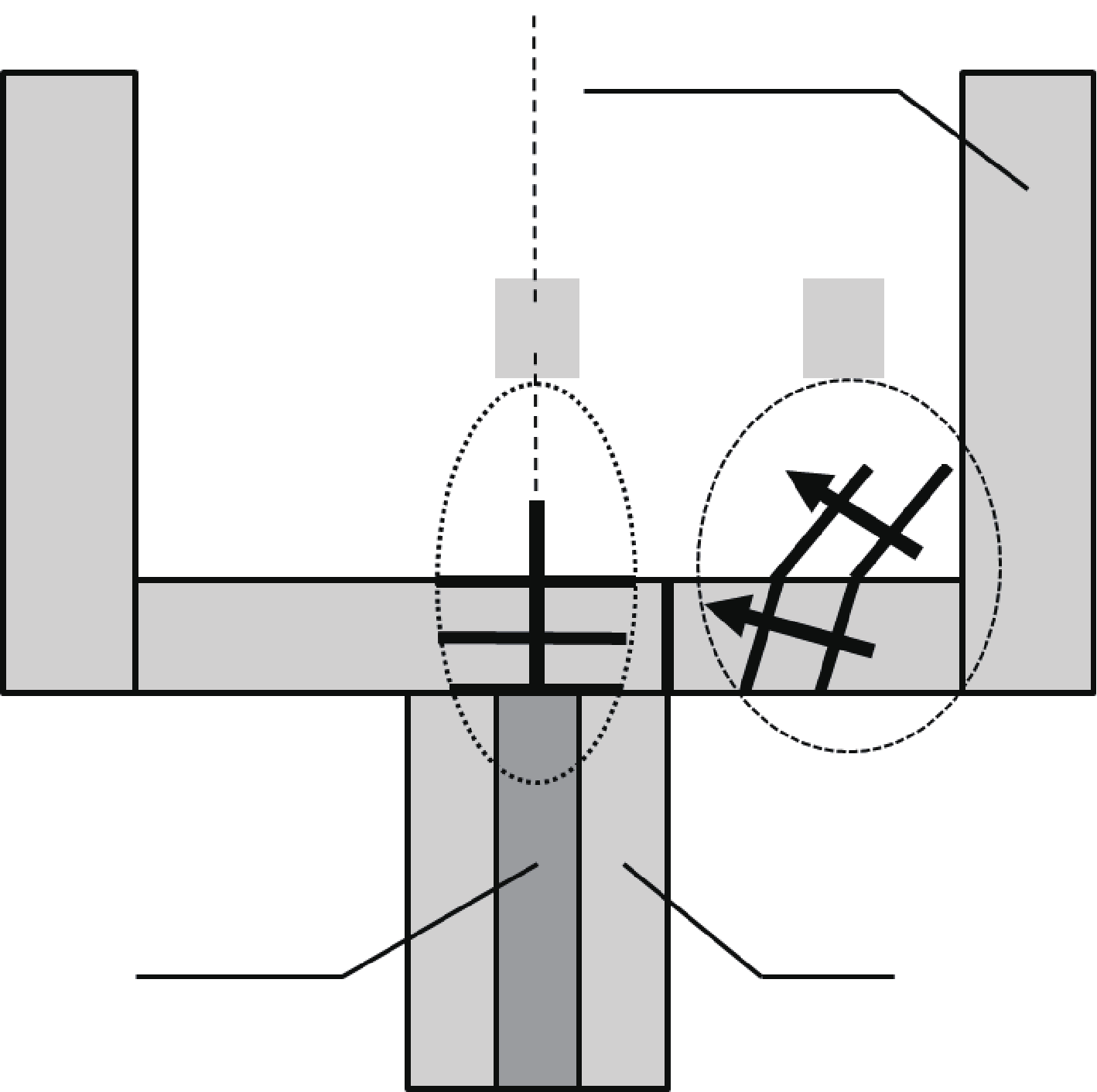
Fig.1 The required temperature distribution and corresponding thermal flux at the bottom of the crucible. A long thermal insulation material surrounds the pedestal under the crucible between regions A and B.
《2.2. Design principle for the thermal system》
2.2. Design principle for the thermal system
To achieve two opposite temperature distributions inside one material, it is necessary to isolate two regions, such as regions A and B. However, it is not easy to achieve this type of isolation because both regions A and B are part of one crucible material. A practical method is to add a long piece of thermal-insulation material under the crucible between regions A and B, as shown in Figure 1. This insulation material can partly isolate the cooling flux inside region A and the heating flux inside region B. It is difficult to completely avoid interaction between regions A and B. To obtain fully single-crystal silicon using the casting technique, a basic principle for the thermal system design is to achieve as much isolation as possible between regions A and B.
《3. Numerical simulation for the crystal-growth and dislocation multiplication processes》
3. Numerical simulation for the crystal-growth and dislocation multiplication processes
《3.1. Simulation for the crystal-growth process》
3.1. Simulation for the crystal-growth process
Inside a 540 mm × 540 mm × 430 mm crucible, the crystal-melt interface and the mass and energy transfer were simulated by numerical modeling. The simulation included convective heat transfer in silicon melt, conductive heat transfer in all solid components, and radiation heat transfer in all enclosures of the furnace. The melt flow in the crucible was assumed to be an incompressible laminar flow. The radiative heat exchange in all radiative enclosures was modeled on the basis of the assumption of diffuse-gray surface radiation. The convective cooling by argon gas was neglected in the computation of thermal fields. The crystal-melt interface was tracked using the enthalpy method [14]. The design of the thermal-isolation structure discussed in Figure 1 was implemented into the modeling.
Figure 2 shows the evolution of the crystal-melt interface and the melt convection during the solidification process. The time interval in Figure 2 is 6000 s. From Figure 2(a) to (e), the shape of the crystal is similar to that of a mushroom, which is a non-artificial growing pattern in nature. The contact angle, which is defined as the angle between the tangent direction of the crystal-melt interface at the triple point of crucible-melt-crystal and the left direction of the crucible bottom (Figure 2), is slightly larger than 90º in Figure 2(a) and becomes obviously larger than 90º in Figure 2(b)−(h). To permit clear observation of the variation in the contact angle, Figure 3 shows the contact angles in Figure 2(a)−(h). All of the contact angles are larger than 90º; the crystal-melt interface therefore marches toward the bottom of the crucible, and polycrystallization nucleation along the bottom of the crucible can be avoided during solidification.
《Fig. 2》

Fig.2 The crystal-melt interface evolution and melt convection during the solidification process.
Figure 2(e)−(h) shows that the crystal-melt interface marches toward the sidewall of the crucible, and polycrystalline nucleation can therefore also be avoided near the sidewall of the crucible. Near the top corner of the crucible, a small ratio of polycrystalline nucleation occurs due to the large thermal dissipation at the top corner of the crucible. This polycrystalline nucleation can be avoided by placing extra thermal insulation around the top of the crucible. Figure 4 shows the volume ratio of single-crystal growth to polycrystalline silicon. It can be observed that the ratio of single-crystal silicon is large, and that the present design produces almost completely single-crystal silicon.
《Fig. 3》
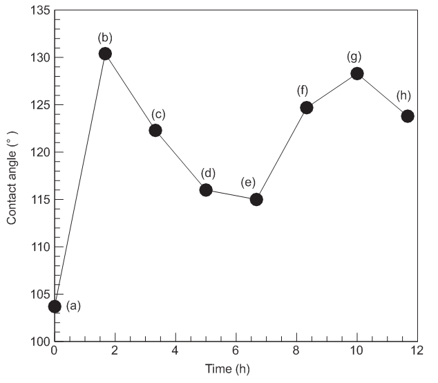
Fig.3 The contact angles between the crystal-melt interface and the left direction of the crucible bottom at different times.
《Fig. 4》
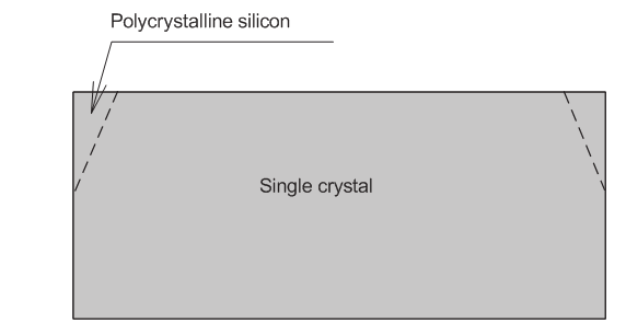
Fig.4 The ratio of single-crystal silicon to polycrystalline silicon.
Therefore, the results of the numerical simulation indicate that the present design is valid and the polycrystalline nucleation along the crucible wall can be avoided.
《3.2. Simulation for dislocation multiplication process》
3.2. Simulation for dislocation multiplication process
After determining the crystal-growth process, the thermal stress during the crystallization process can be simulated. We made two assumptions for the thermal stress calculation: first, that the stress is always equilibrium; and second, that the shape of the material is kept constant during the thermal process because of small practical deformation of the material.
Figure 5 shows the thermal stress during the crystallization process. A maximum cooling flux of 7.0 kW.s−1 is provided from the pedestal. Parts (a)−(d) of the figure show the initial growth from the silicon seed. Parts (e)−(h) of the figure show that the crystal grows with a large curvature near the crucible bottom.
《Fig. 5》
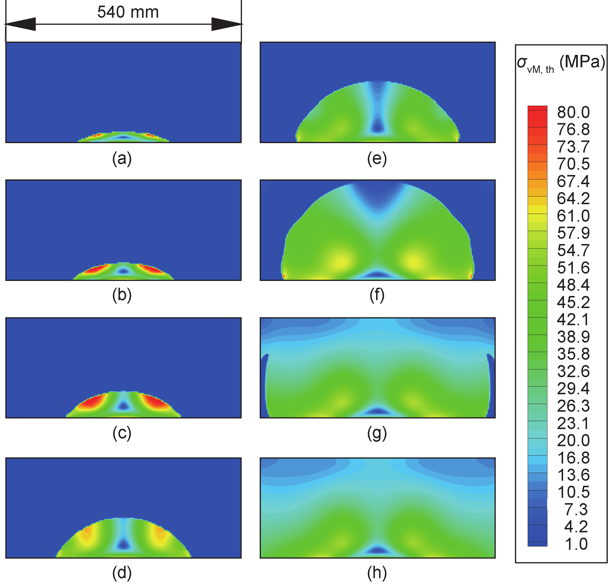
Fig.5 The von Mises stress distribution during crystal growth for the new shape of monocrystalline silicon.
A decrease in the maximum thermal stress at the initial stage can be achieved by providing a small cooling flux, which can be derived from careful observation of the thermal stress in Figure 5. At the initial stage of crystal growth shown in Figure 5(a)−(c), the thermal stress along the crystal-melt interface gradually increases because of an increase in the curvature of the interface. However, when the crystal grows, the thermal stress along the crystal-melt interface gradually decreases, although the curvature becomes larger than that during the initial stage. This contrast in behavior can be explained by the relationship between thermal stress and thermal flux, because it is well-known that the thermal stress is determined by the temperature gradient and that the temperature gradient is directly proportional to the thermal flux [15]. Thus, the amplitude of the thermal stress can be determined by the amplitude of the thermal flux. In the present case, almost all of the thermal flux is provided by the pedestal, which is located at the center of the crucible bottom. The total thermal flux provided by the pedestal determines the amplitude of the thermal flux at every crystal-melt interface point. If the total cooling flux at the pedestal is kept constant, when the area of the crystal-melt interface is small during the initial stage, the cooling flux at every crystal-melt interface point is relatively large. When the crystal grows, the total area of the crystal-melt interface becomes large and the cooling flux at every crystal-melt interface point becomes relatively small. Therefore, the thermal stress is relatively large at the initial stage, and relatively small at the later stage. Consequently, an effective method to decrease the thermal stress at the initial stage is to reduce the total cooling flux at the pedestal.
After the thermal stress is obtained, the dislocation density can be simulated using the Alexander-Haasen model [12]. Figure 6 shows the dislocation evolution at different stages. The order of dislocation density inside the global crystal is 105 cm−2, which is larger than that of the single-crystal silicon produced by the Czochralski (Cz) and floating zone (FZ) methods. However, the real value of the dislocation density might be much lower than this value, because the present Alexander-Haasen model does not include the annihilation effect of dislocations. Furthermore, this new growth can effectively decrease the possibility of cross-slip because the dislocation marching direction is divergent from the seed during crystal growth.
《Fig.6》
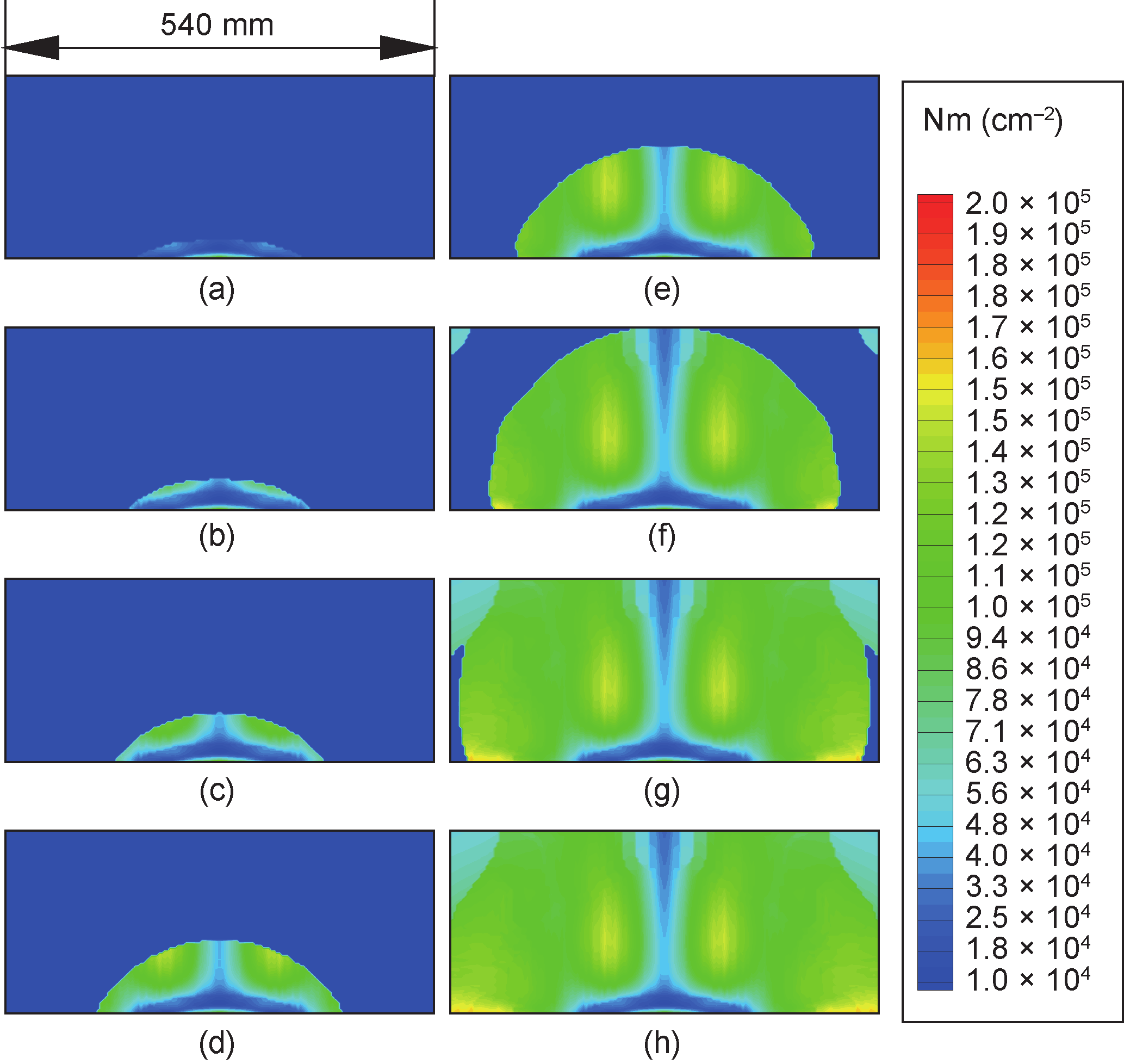
Fig.6 The dislocation density distribution during the crystal-growth process.
The dislocation distribution also demonstrates the importance of the initial stage. The dislocation density gradually increases along the crystal-melt interface during the initial stages, as shown in Figure 6(a)−(c). During later stages, shown in parts (d)−(e) of the figure, the dislocation density does not increase as much and only maintains the order of the previous solidified surface, due to the projection effect from the previous solidified surface to the new solidified surface. Thus, if only the initial dislocation is controlled, the global dislocation inside the crystal may decrease.
Therefore, the results of the dislocation simulation indicate that the present design is valid and that dislocation density can be controlled to a small value inside the global crystal if a small initial cooling flux is imposed.
《4. Experimental resultsAfter Ref. [16] with permission from Elsevier.》
4. Experimental resultsAfter Ref. [16] with permission from Elsevier.
According to our design, we restructured a large-size industrial furnace that was originally designed for multicrystalline silicon production. In the new furnace, a quartz crucible coated with a layer of Si3N4 was placed on a carbon susceptor at the center of the furnace. The size of the crucible was 540 mm × 540 mm × 430 mm. A silicon seed with a diameter of 20 mm and a thickness of 20 mm was placed at the center of the crucible bottom. Initial raw material with a mass of 120 kg was charged into the crucible in order to grow a crystal with a height of 200 mm. The pressure of argon gas in the furnace could be controlled from 1 Pa to 1 atm (1 atm= 101.325 kPa). To realize the mushroom-shaped interface, a thermal flux was supplied from a heater and removed from the pedestal. The thermal flux was carefully controlled in order to melt only the raw material, leaving the seed unmelted. After completely melting the raw material, the heater power was gradually reduced until solidification occurred, followed by cooling to room temperature.
Figure 7 compares the newly grown crystal with a crystal grown in the old furnace. The crystal grown in the old furnace, shown in Figure 7(a), exhibits a very dirty surface full of carbon and nitride impurities; in contrast, the crystal grown in the new furnace, shown in Figure 7(b), exhibits a very clean surface. The clean surface is due to our cover design as demonstrated in our previous study [17]. The reduction of impurities can greatly decrease the nucleation of precipitations inside the crystal, reducing the possibility of dislocation generation. The reduction of dislocations is extremely helpful for the realization of our single-seed casting technique.
《Fig. 7》
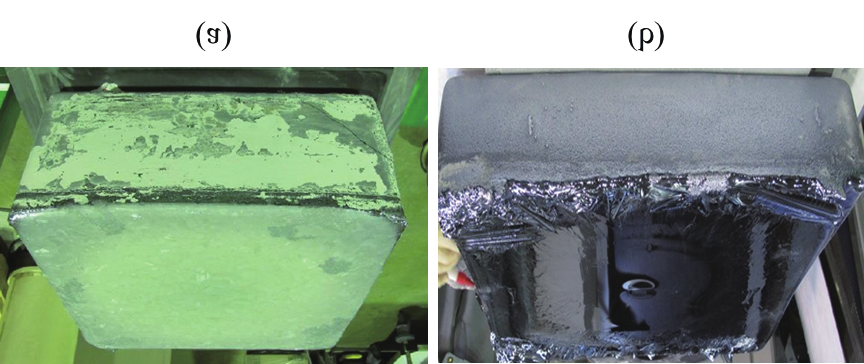
Fig.7 A comparison of crystals grown in the (a) old and (b) new furnaces.
To examine the detail of the crystal, we took a wafer-size slice with the dimensions of 156 mm × 156 mm from the top surface of each crystal. Figure 8 compares the two slices. The slice in Figure 8(a) is from monocrystalline silicon grown by our technique. The slice in Figure 8(b) is from multicrystalline silicon grown by a conventional casting technique. Our technique produces an ingot without grain boundaries, while the conventional technique produces an ingot with many grain boundaries. Therefore, the present design successfully grows a single crystal in an ingot.
《Fig. 8》

Fig.8 Photographs of silicon ingot surfaces for (a) monocrystalline silicon and (b) multicrystalline silicon.
We used X-ray topography (XRT) and etch-pit observation to examine the quality of the crystals grown by our technique. Figure 9 presents an XRT image of a vertical cut from the center of the ingot. The interface between the seed and the grown crystal is visible as the horizontal line in the middle. The straightlines, which correspond to slip dislocations or twins, are introduced from the interface as well as from the top surface. The dislocations generated at the interface may originate from the rough seed surface.
《Fig. 9》
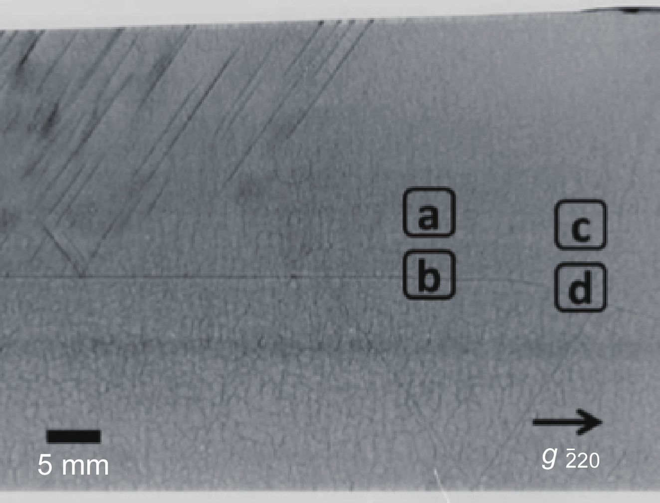
Fig.9 An XRT image of a vertical sliced sample from monocrystalline silicon grown by our technique. The labels a, b, c, and d represent locations where etch-pit observation images were taken (see Figure 10).
The etch-pit observations in Figure 10 provide detailed information. These images were taken at the corresponding areas marked in Figure 9. We can see that from bottom to top, the dislocation density was gradually reduced; this is quite superior to the multiseed casting method, which produces a gradually-increasing dislocation density. The dislocation density is on the order of 104−105 cm−2, which is also much less than that of the multiseed casting method.
Kyocera Solar Inc. tested solar cells developed from our single-seed casting technique. The average efficiency of the entire ingot is 19.6%, which is much higher than the performance of popular high-performance multicrystalline silicon [11]. The difference in efficiency between solar cells made from the top part and those made from the bottom part of the ingot is quite small. Therefore, the quality of the entire ingot fabricated using our technique is quite high and homogeneous. The single-seed casting technique presented here is very promising for application to future low-cost and high-efficiency solar cells.
《Fig. 10》
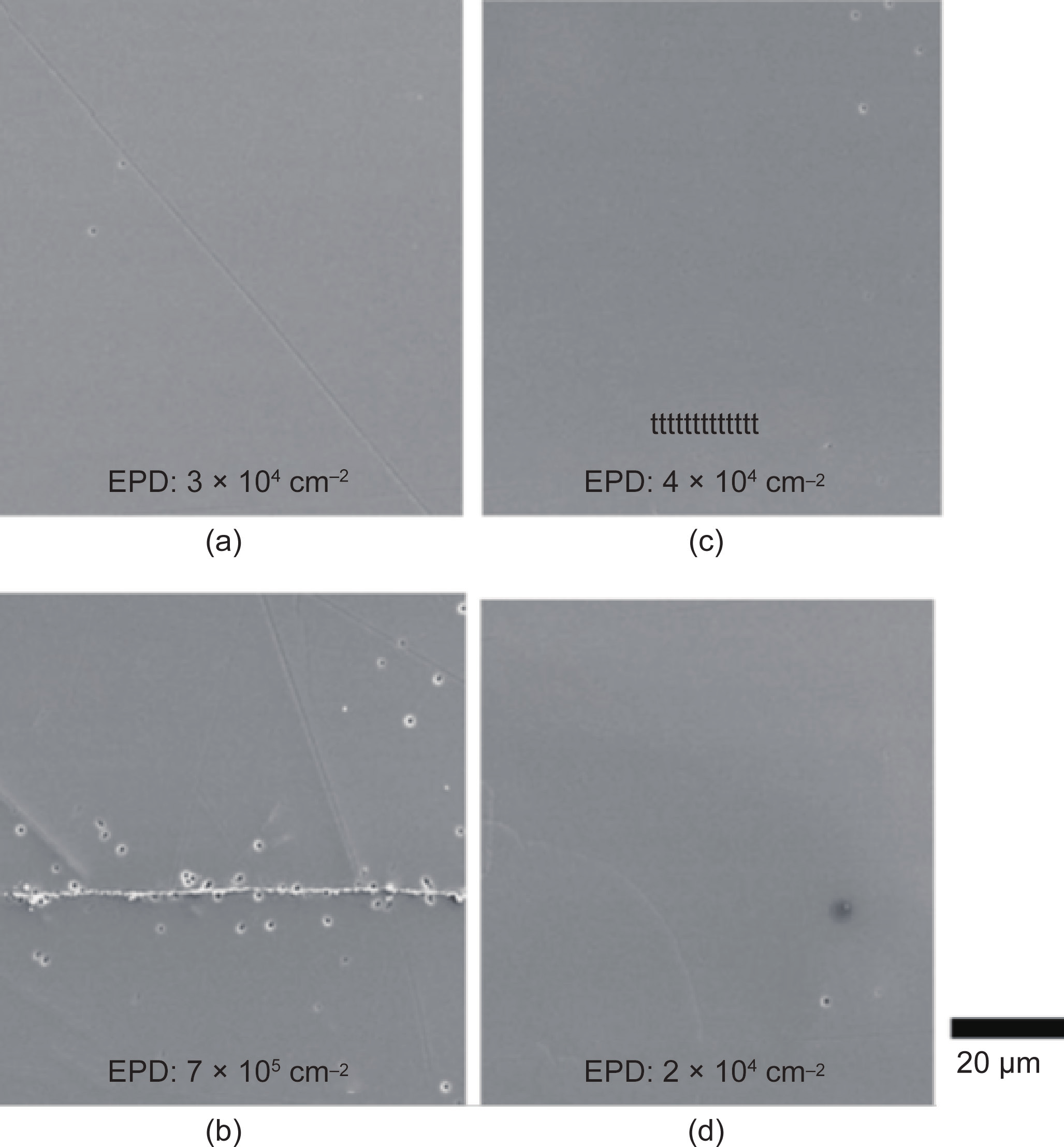
Fig.10 Scanning electron microscope (SEM) images after Secco etching of vertical sliced samples from monocrystalline silicon.
《5. Conclusions》
5. Conclusions
We proposed a single-seed casting technique for producing low-cost and high-quality monocrystalline silicon for solar cells. This technique can grow a large-size and fully single-crystal ingot that exhibits superior performance to ingots prepared using the popular high-performance multicrystalline and multiseed casting techniques.
To realize this technique, two challenges—polycrystalline nucleation on the crucible wall and dislocation multiplication inside the crystal—needed to be solved. To avoid polycrystalline nucleation on the crucible wall, the crystal-melt interface must march toward the crucible wall; to reduce dislocation multiplication, the initial cooling flux from the pedestal must be controlled to a small value.
《Acknowledgements》
Acknowledgements
This work was partly supported by the New Energy and Industrial Technology Development Organization (NEDO) under the Ministry of Economy, Trade and Industry (METI), Japan.
《Compliance with ethics guidelines》
Compliance with ethics guidelines
Bing Gao, Satoshi Nakano, Hirofumi Harada, Yoshiji Miyamura, Takashi Sekiguchi, and Koichi Kakimoto declare that they have no conflict of interest or financial conflicts to disclose.


 京公网安备 11010502051620号


