
《 1.Introduction》
1.Introduction
Photovoltaic (PV) technology, which directly generates electricity from sunlight, is quickly becoming a major player in the future clean energy economy. Solar PV is efficient, quiet, modular, easy to install, and requires little maintenance. Given suitable location and planning, electricity production by PV systems can be even cheaper than conventional generation from fossil fuels [1,2]. The costs for PV systems are dropping continuously and their energy generation price is not affected by future fuel price increases.
Although advances in technology and mass production of conventional silicon (Si)-wafer-based solar modules have led to amazing price reductions, this technology is subject to fundamental limitations, especially regarding materials consumption, production speed, and features such as flexibility and form factor.
PV modules based on Cu(In,Ga)Se2 (CIGS) thin-film semiconducting materials have already entered the market at similar or even lower costs than traditional silicon modules [1], but without yet profiting from the same economies of scale. Significant cost reductions are therefore to be expected once this technology is at a similar scale as conventional silicon PV. In this contribution, we focus on the CIGS technology.
《2.General comparison of CIGS-based thin-film and Si-waferbased PV technologies》
2.General comparison of CIGS-based thin-film and Si-waferbased PV technologies
A solar cell is basically a large-area semiconductor diode. The silicon technology applies diffusion-based doping techniques, similar to the electronics industry, on monocrystalline or multicrystalline wafers to create the p–n junction. The silicon material requires a high degree of purity and the processing steps from quartz sand to semiconducting wafers are very energy intensive. In order to reduce materials consumption, modern solar silicon wafers are very thin— about 120 µm in thickness of high-purity silicon. Process optimizations such as the reduction of materials loss due to sawing the wafers or the increase of efficiency by special patterning and passivation strategies lead to incremental reductions in the cost structure while introducing more complexity into the production line. The machinery must employ careful handling procedures to manipulate these fragile pieces. One advantage of the Si-wafer-based PV technology is that the individual solar cells can be sorted by performance and the modules are assembled from a set of practically identical cells. The other advantage is the advanced commercial maturity of the technology.
In comparison, the materials for thin-film solar cells are direct semiconductors with a much higher absorption coefficient than silicon. For this reason, 1–3 µm of absorber material is sufficient to absorb and convert all of the incoming sunlight. Such a thin layer is not mechanically stable, so it is coated on a substrate. A typical substrate is window glass, but substrates such as a polymer or metal foil are also suitable for the production of lightweight and flexible solar modules. Despite the energy-intensive steps of glass production and vacuum-coating techniques, the energy payback time for CIGS-based thin-film PV modules is significantly lower than that of conventional silicon modules: for example, 0.78 year compared to 2.12/1.23 years for mono-/multi-Si (calculated for module production in China, 1700 kW·h·m−2 solar irradiation per year) [3].
CIGS-based thin-film PV is produced directly in module form by means of the monolithic integration technique. Three patterning steps separate the front and back contacts between cells and provide an interconnection between them so that the module has a uniform “pinstripe” appearance. The “stripes” distinguish the individual cells, which are connected in series, as shown in the example in Fig. 1. The patterning layout can be easily modified to generate a wide range of voltage outputs for the module or to create a module with an unusual shape. This feature can be particularly attractive for building or product integration. The entire CIGS module is produced in one factory (glass in—module out).
《Fig. 1》

Fig. 1. A 30 cm × 30 cm CIGS module on glass produced in the laboratory pilot line of Centre for Solar Energy and Hydrogen Research Baden-Württemberg.
In sum, thin-film technologies in general and CIGS in particular have a high potential for reducing the cost of clean energy generation by solar PV. Compared with the standard Si-wafer-based PV technology, CIGS has a much lower materials requirement and requires less energy to produce. The production is highly automated and requires fewer machines than silicon technology production, if the entire chain is considered. Since the CIGS modules are produced in one factory, the production has a high degree of local added value and the factories can be profitable even on a relatively small scale. As the CIGS technology matures further in the future and as the module efficiencies increase to reflect advances in research and development, the cost advantage will continue to progress.
《3.CIGS technology basics》
3.CIGS technology basics
The CIGS technology is named after the CIGS absorber layer. It is typically grown on a molybdenum (Mo) back contact supported by a glass substrate. The p–n junction is formed by applying a buffer/ window layer combination of cadmium sulfide (CdS), undoped zinc oxide (ZnO), and aluminum (Al)-doped ZnO (or alternative materials). The latter is a transparent conducting oxide and serves as the front contact. The Mo and ZnO layers are sputtered while the CdS layer is deposited in a chemical bath. Laboratory cells employ a metallic grid for reduced contact resistance, and an anti-reflection coating may also be applied. Some cell designs also include a barrier for alkali elements either below or integrated into the Mo back contact. Alkali elements such as sodium (Na) are essential to achieving high efficiencies and are generally introduced by diffusion from the glass substrate. If a barrier is applied, or if the substrate does not contain alkali elements, then an alternative alkali source is required for high efficiencies, such as a sodium fluoride (NaF) layer or a Na-doped Mo layer (Mo:Na) [4].
Fig. 2 illustrates a cell layer stack with typical thicknesses and a scanning electron microscope image of the cross-section. The sickleshaped crystallite growth of the Mo and ZnO layers, which can be found at the top and bottom of this cross-section, results from moving the substrate under a sputter target in an inline sputter-coating machine. The multicrystalline grain structure of the CIGS layer is also apparent, with larger and smaller grains and some voids. Not all grain boundaries are perpendicular to the layer plane.
《Fig. 2》
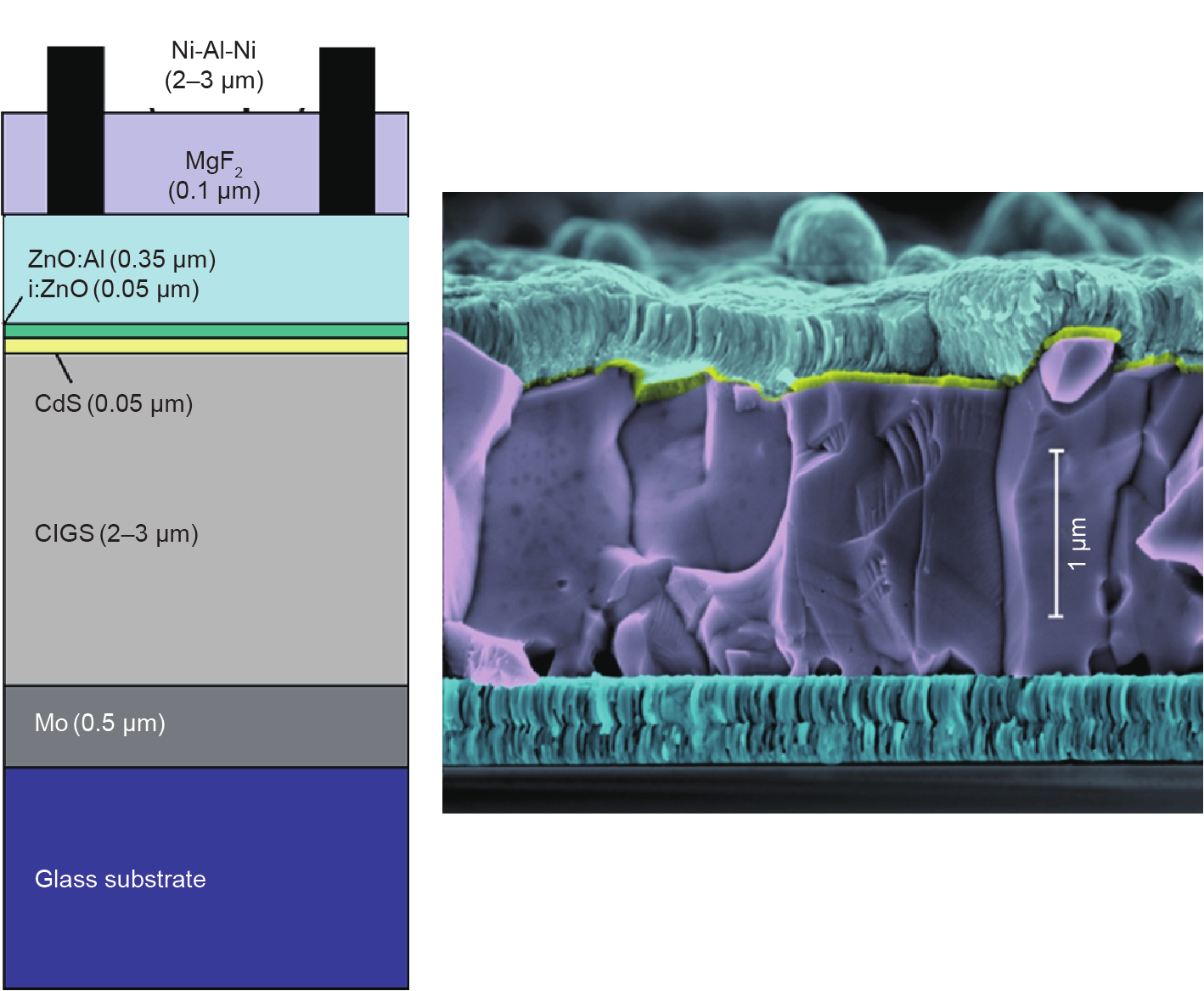
Fig. 2. Schematic structure of the solar cell (left) and cross-section scanning electron microscope image of a standard CIGS solar cell (right).
There are two major approaches to the deposition of the CIGS layer: co-evaporation and sequential processing [5,6]. In the co-evaporation process, all elements are thermally evaporated in a vacuum process and the CIGS layer forms directly on the Mo-coated substrate. In the so-called sequential process, the metals copper (Cu), indium (In), and gallium (Ga) are first deposited, such as by sputtering or electrodeposition. The metal layers are then converted to CIGS in a sequential selenization process. This procedure is often finalized with a sulfurization process to increase the band gap near the interface. Both methods have been shown to lead to high cell efficiencies [6,7].
At the Centre for Solar Energy and Hydrogen Research BadenWürttemberg (ZSW), we have developed the inline co-evaporation process for CIGS to a level that is suitable for commercial implementation, by exploiting the inherent advantages of the coevaporation technique to coat CIGS in one machine and with flexibility of composition control [8]. The thermal evaporation line sources are arranged to provide favorable growth conditions and composition profile in the layer. For example, the Ga content (which is directly related to the band gap) is increased toward the back and front of the film in order to reduce back-surface recombination and increase the built-in voltage, respectively. The very-high-efficiency cells are produced in a static system in which the elemental fluxes can be carefully controlled [9]. Fig. 3 illustrates the differences between static and inline coating processes in laboratory and industrial configurations. The schematic shown in Fig. 3(a) represents the static process, in which the substrate is in one location. The elemental fluxes are adjusted over time during the CIGS deposition in order to achieve a high-quality multicrystalline layer and a favorable Gacontent profile. This method allows the highest flexibility but the lowest throughput. Thus, it is used for research purposes only. In an inline deposition system such as that represented by Fig. 3(b) and Fig. 3(c), the substrate moves through the system. Each evaporation source is set to a constant flux, but its position and orientation is carefully designed to reproduce a favorable composition profile during the film growth. The ZSW design enables coating from top to bottom, so that the substrates are well-supported by the conveyance system. Our industrial partner Manz AG/Manz CIGS Technology GmbH (MCT) has further developed the CIGS coating technology to the level of a truly industrial system that is designed for large substrates (~1 m2), with a very fast cycle time (as low as 2 min).
《Fig. 3》
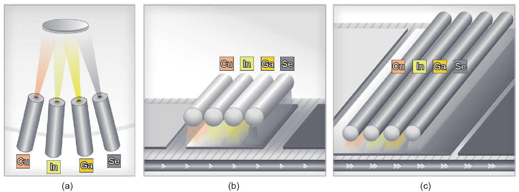
Fig. 3. Configurations for CIGS deposition by co-evaporation. (a) Static configuration, in which fluxes are regulated over time; (b) inline configuration, in which sources are configured to provide correct constant fluxes to a moving substrate; (c) industrial configuration, which coats larger substrates at faster speeds.
《4.Advances in CIGS cell efficiency》
4.Advances in CIGS cell efficiency
Continuous research and development have led to AM1.5 cell efficiencies for CIGS of up to 22.6%, as certified in 2016 [10]. Despite this high efficiency level, the CIGS-based PV technology has not yet attained its full potential. If all loss mechanisms were addressed at the same time, an efficiency level approaching 30% would be technically feasible [11]. In the following discussion, we examine the status of the highest efficiency CIGS solar cells and consider approaches for further improvement.
The CIGS solar cell efficiency of 22.6% set a world record as the highest of any thin-film technology, and is even higher than that of multicrystalline silicon (21.9% [12]). It was made with a layer sequence similar to the one shown in Fig. 2. By purely optimizing efficiency rather than costs, a very-high-efficiency cell was developed with a slightly thicker CIGS absorber layer than a commercial product. A separate high-efficiency cell production line at ZSW is dedicated to these processes and every step is highly optimized. Recent progress in efficiencies exceeding 21% became possible through a major modification after the CIGS growth process. The so-called “post-deposition treatment” (PDT), with alkali fluorides evaporated in a selenium (Se) atmosphere, adjusts the surface composition to lower Cu and Ga content and increase the content of the alkali element, such as potassium (K) or rubidium (Rb) [10]. This treatment of the interface between CIGS and CdS influences the quality of the p– n junction and is therefore decisive for the resulting device performance. The PDT process can significantly increase the open-circuit voltage, an effect that is most likely a result of reduced charge carrier recombination in the interface region [13]. An additional positive effect is that the minimum thickness required for the CdS layer is reduced, which is potentially related to a reduction of Cu concentration that has been observed at the surface. Since photons absorbed in the CdS layer do not contribute to current generation, a thinner CdS layer directly contributes to improved efficiency. Apparently, the PDT-CIGS surface enables a more uniform CdS growth in the initial phase [14,15]. A schematic of the PDT process and its effects is shown in Fig. 4.
《Fig. 4》
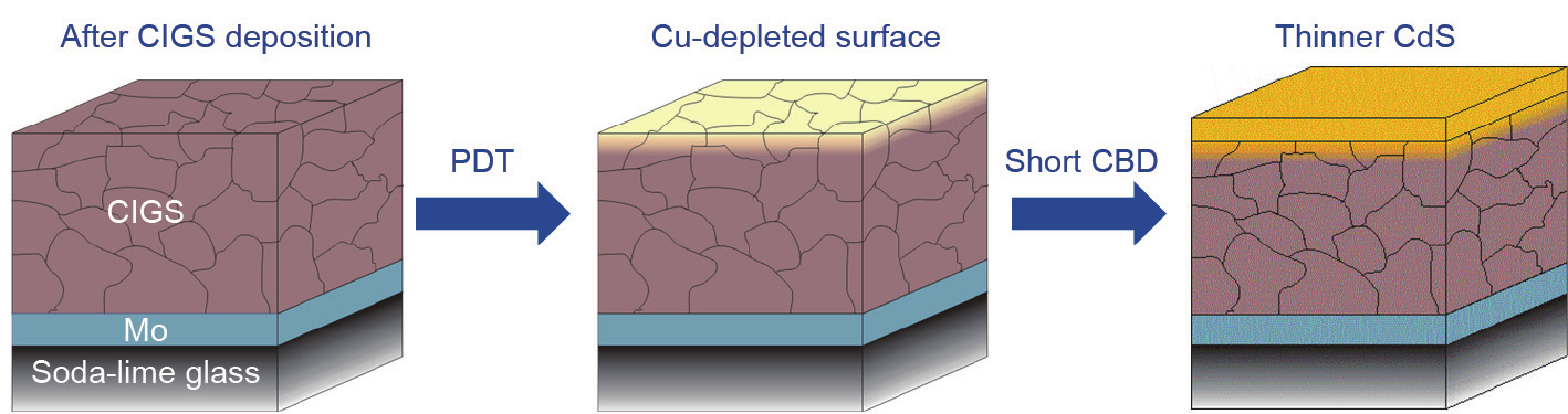
Fig. 4. Schematic description of the PDT process and its effects. CBD: chemical bath deposition.
Another improvement in current generation can be achieved by replacing the thin non-doped ZnO layer with (Zn,Mg)O, as was done in the current world-record CIGS cell with an efficiency of 22.6% (see Fig. 5 for details) [7]. (Zn,Mg)O has a slightly higher band gap and therefore transmits more ultraviolet photons to the CIGS absorber layer. It is regularly used instead of non-doped ZnO in combination with a Zn(O,S) buffer (instead of CdS) [16]. Zn(O,S) is an attractive buffer material due to its larger band gap as compared with CdS, which reduces optical losses in the buffer layer. An additional bonus is the exclusion of cadmium (Cd) from the device structure. The world record for the efficiency of a Cd-free CIGS cell is currently 22.0% [17]. Thus far, the best certified ZSW cell with Zn(O,S) buffer has an efficiency of 21.0%, which is markedly lower than the 21.7% efficiency of the analogous cell with a CdS buffer [14]. The performance reduction with Zn(O,S) buffer is most apparent in the open-circuit voltage. Significant potential for efficiency improvement is accessible if the voltage can be improved with Zn(O,S) or other buffers that enable better conversion of photons with wavelengths between 300 nm and 500 nm (compared with the external quantum efficiency in Fig. 5).
《Fig. 5》

Fig. 5. (a) Current-voltage and (b) external quantum efficiency (EQE) curves of the 22.6% cell, as certified by the CalLab at Fraunhofer ISE.
With these current achievements, CIGS is not only an alternative PV technology option that promises lower production costs than the standard silicon PV technologies; it is also a serious high-efficiency competitor on the market. This fact is demonstrated by a comparison of the record efficiency development of CIGS with those of two of the PV market’s most prominent players: monocrystalline silicon and multicrystalline silicon. Monocrystalline silicon has made hardly any progress in the past 20 years. In fact, CIGS has been able to surpass multicrystalline silicon in the past five years and is now fast approaching the efficiencies of monocrystalline silicon. Moreover, as Fig. 6 shows, in the past months, the ZSW CIGS high-efficiency cell production line was able to produce nearly 700 cells with efficiencies near the level of the current efficiency world record for thinfilm solar cells. This is an impressive number for a low-throughput process, and it shows that the increased development speed of CIGS technology has not yet plateaued—rather, it is likely to continue. With such promising prospects at hand, CIGS technology truly appears to be a serious contender in the PV market of the near future.
《Fig. 6》
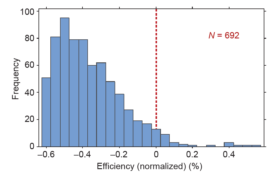
Fig. 6. Histogram of the frequency of high-efficiency CIGS solar cells made by ZSW, normalized to the current 22.6% record cell (efficiency normalization and corrections are calculated due to differences in the state of the cells compared regarding the presence of an antireflective coating, and due to different grid designs in the data used).
《5.From cell to module》
5.From cell to module
A solar cell delivers 500–800 mV of voltage, depending on its exact composition and design. The current depends on the cell area and the illumination. In order to produce meaningful amounts of electrical energy, larger areas are needed and the cells must be connected electrically to generate higher voltages. The thin-film technology enables monolithic interconnection of the cells since patterning steps can be performed between coating steps so that the production line directly generates PV modules. The standard method of monolithic integration involves three patterning steps: first, separation of the cells at the back contact by opening the Mo layer; second, an interconnection by opening the CIGS layer, so that an electrical contact between the front and back contacts is created during the subsequent processing steps; and third, a final patterning step for the front side cell separation. The module voltage is thus determined by the number of cells in series connection.
The inline coating of CIGS was described above. The sputtered contact layers can be easily coated in a commercially available inline system. The CdS layer is typically coated in a batch-type chemical bath deposition process. Industrial solutions for this step have already been developed. Additional steps required for a commercial product include attaching contact tapes, laminating to a front glass, and integrating a junction box and connectors. The glass-glass assembly is mechanically sturdy, so a frame is optional.
Obviously, the highest efficiencies have been achieved at cell level. On a module level, there are inherent losses due to inactive areas for the monolithic interconnection and series resistance losses. The series connection also limits the module current to that of the lowest performing cell. Spatially uniform processing conditions are therefore key to achieving high efficiencies for large-area modules. Fig. 7 illustrates the development of the highest published conversion efficiencies for the CIGS technology at cell and module level over time. The cell data is based on the National Renewable Energy Laboratory (NREL) PV efficiency chart [18], with 22.6% as the highest value. The recently reported record efficiency of 21.9% for the multi-Si cell is included for comparison [12]. The values for small modules were reported for areas up to 1000 cm2 and the full-size modules are in the range of 7000 cm2, with record aperture efficiencies of 19.2% and 17.9%, respectively [19,20]. Additional historical information about the research developments leading to improved cell efficiency is included in the figure. New research developments lead to fast efficiency improvements, while process optimization and technical developments lead to slower incremental efficiency improvements. The modules will always have a lower efficiency than the best cells due to the losses described above and due to the time lag in implementing new research developments at a module level. The difference in the efficiencies of small modules and fullsize modules is not as large. This plot clearly illustrates the stilllarge potential for progress in efficiencies at both the cell and module level, since cell efficiencies have not yet plateaued and module efficiencies do not yet fully reflect recent developments. Indeed, the PDT process has already been implemented in industrial inline CIGS co-evaporation coating plants, and this improvement should soon be reflected in their average efficiencies.
《Fig. 7》

Fig. 7. Development of champion CIGS efficiencies at cell and module level over time, based on the NREL PV efficiency chart [18] and individual publications. The recent multi-Si record cell is included for comparison [12].
《6.Production and applications》
6.Production and applications
ZSW operates a laboratory pilot line that is capable of producing encapsulated modules up to 30 cm × 30 cm in size. This technology is licensed to our industrial partner MCT, which runs a 6 MW research and development line with full-size machinery. The CIGSfab of the Manz AG is a complete production line for CIGS modules based on the ZSW CIGS technology. Joint ventures with Chinese partners have recently invested in CIGS factory lines and their future development. The production of CIGS modules is therefore expected to increase dramatically in the near future.
A typical full-size CIGS module from Manz AG is 60 cm × 120 cm in area, with a uniform black appearance that is especially attractive for building integration purposes. An example is shown in Fig. 8, which shows CIGS modules being used as facade elements on the new ZSW building in Stuttgart, Germany.
《Fig. 8》

Fig. 8. CIGS modules as facade elements on the ZSW building in Stuttgart, Germany.
CIGS modules from ZSW and Manz AG, as well as those from other producers and technologies, have been regularly and rigorously tested throughout the two-decade history of our outdoor testing site in Widderstall, Germany. The results are compared with meteorological data and correlated with laboratory testing data, such as with flasher measurement of the current-voltage curves and with climate chamber testing. Fig. 9 illustrates an example of outdoor testing on a CIGS module from Manz AG over two years. The data were acquired every minute and converted to the corresponding values under standard test conditions (STC) using measured meteorological data such as intensity of sunlight and temperature. The darker points represent the five-day median of the data sets, and the black diamonds indicate additional flasher values attained by indoor testing. The flasher values validate the STC-adjusted data well. The stability of the CIGS module is demonstrated over the two-year outdoor testing period.
《Fig. 9》
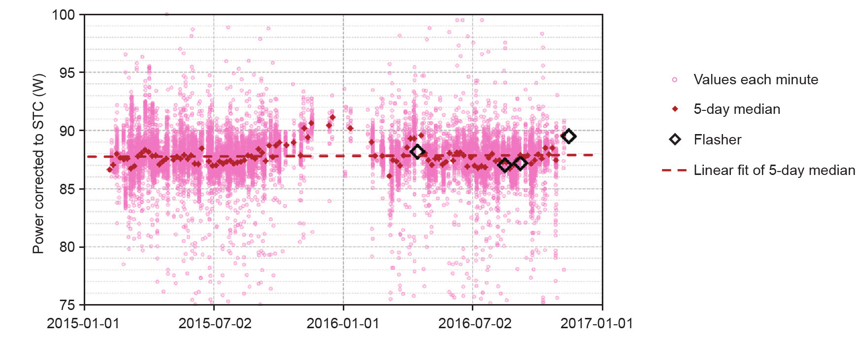
Fig. 9. Example of outdoor testing of a CIGS module. Data is converted to STC values based on measured meteorological data and compared with indoor flasher values. Performance stability is demonstrated over a two-year time span.
《7.Lightweight and flexible》
7.Lightweight and flexible
Although glass is a convenient substrate with many positive characteristics—such as its smooth surface, sufficient temperature stability, ability to act as a source of alkali elements, and electrical insulation—it is rigid, fragile, and heavy. Solar modules on a flexible substrate such as a polymer or metal foil (Fig. 10) have several additional advantages: They can be molded to the curved surface of a building or an object such as a motor vehicle; they are very lightweight compared with a module on glass, and therefore require less mechanical support for mounting; they can be rolled up for storage or for deployment in a satellite; and they can be produced in fast roll-to-roll machinery. Due to the comparably low heat capacitance of thin foils, the warming-up phase and cooling time can be rather short, resulting in compact roll-to-roll coating machines and high web speeds. In some cases, the substrate itself may even be cheaper or have a lower energy payback time than glass. Several manufacturers already focus on the production of flexible CIGS cells and modules.
《Fig. 10》
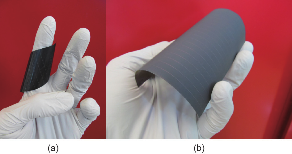
Fig. 10. (a) Flexible CIGS module on polyimide foil with strong curling behavior;(b) steel foil with very low curling behavior (module is intentionally bent to show high flexibility).
The efficiencies of flexible CIGS solar cells have typically been lower than those of cells on glass, although a cell with an efficiency of 20.4% has already been achieved [21]. There are several reasons for this lag, one of which is simply the fact that more research has been performed in the field of “CIGS on glass” and that rigid modules are more suitable for large-scale deployment. Depending on the choice of flexible substrate, different challenges must be solved for highefficiency CIGS solar modules. We will distinguish between polymer and metal foil substrates. Some solutions require modification to the CIGS process, mostly due to temperature constraints, and some require additional functional layers such as diffusion barriers.
The CIGS coating process, as developed for glass substrates, employs moderately high temperatures above 600 °C. This temperature is beneficial for large grains and for a high semiconductor quality in the CIGS layer. The glass also softens slightly, which facilitates the release of beneficial alkali elements such as Na from the glass to the CIGS layer. Despite the softening, the glass substrate has sufficient mechanical integrity to withstand the coating process, especially in the top-down coating configuration. The most temperature-stable polymer foil—polyimide—can only withstand temperatures up to 450 °C for a certain period before becoming brittle. One necessary modification to the CIGS process is therefore a reduction of thermal impact to the substrate for polyimide. In a roll-to-roll system, the web is under tension while being heated in the CIGS process. Depending on the manufacturer’s recipe, the resulting product may be prone to significant curling behavior after removal from the machine (see Fig. 10(a)). In order to prevent layer detachments or film cracks, the coefficient of thermal expansion of the web and those of the functional layers should be as close as possible.
A metal foil can withstand the typical CIGS processing temperatures, or even enable higher temperatures, but diffusion of detrimental elements, such as iron (Fe), from the substrate may occur. Therefore, various diffusion barriers have been developed [22]. Additional beneficial features of the diffusion barrier may include providing insulation from the metal contact [22,23]—for example, when monolithic integration is employed—and generating a smooth surface for the subsequent layer depositions, starting with Mo.
A further modification is based on the need for a supply of alkali elements, since they are not released by the polyimide or metal foil. Different methods have been developed to supply alkali elements when they are not available from the substrate. They can be provided by a precursor layer such as NaF, or included as part of the back contact such as Mo:Na [4]. They can also be provided as an extra component during the CIGS coating process, such as by co-evaporating NaF with the other elements. Finally, a PDT [24] subjecting the CIGS to an atmosphere containing the alkali elements is also possible, as are combinations of the abovementioned options. A further option is to dope the insulating diffusion barrier layer with alkali elements so that these can diffuse into the CIGS layer during the CIGS layer growth, as has been realized by Na-doped sol-gel layers [22] or enamel layers [23]. Cells on enameled steel substrates demonstrated even higher efficiencies than cells on standard glass substrates [23,25].
《8.Summary》
8.Summary
In a relatively short time span of roughly two decades, the CIGSbased PV technology has progressed from an interesting scientific research topic to a potential major player in clean energy generation. Although commercial activities are still limited, they already indicate electricity generation costs that are competitive with the highly mature Si-wafer-based PV technology. Standardization of equipment and experience gained from a ramp-up of CIGS-based PV production will further reduce production costs, since this potential has not yet been accessed. At the same time, new developments in efficiency improvements are still continuing and are still to be implemented at a commercial module level. Since efficiency improvements translate directly into a reduction of electricity generation costs, the CIGS technology will only become more attractive as these developments are realized. CIGS-based PV technology is also attractive for applications in aesthetic building integration and for curved surfaces with a flexible product. Future developments are moving toward a flexible substrate to enable novel production methods, and also to achieve practical features such as reduced weight for the system. Although the CIGS-based PV technology is already commercially viable, current and continuing research and development activities will secure its place in the future energy system.
《Acknowledgments》
Acknowledgments
The authors expressly acknowledge Philip Jackson for his intense efforts to drive the CIGS efficiency development forward, and for his provision of the statistics and critical discussion of the manuscript. We also gratefully acknowledge our funding by the German Federal Ministry for Economic Affairs and Energy (BMWi), the German Federal Ministry of Education and Research (BMBF), the German State of Baden-Württemberg, and the European Union.
《Compliance with ethics guidelines》
Compliance with ethics guidelines
Michael Powalla, Stefan Paetel, Dimitrios Hariskos, Roland Wuerz, Friedrich Kessler, Peter Lechner, Wiltraud Wischmann, and Theresa Magorian Friedlmeier declare that they have no conflict of interest or financial conflicts to disclose.


 京公网安备 11010502051620号


