

《1. Introduction》
1. Introduction
Classical philosophy described the process of human thinking as the mechanical manipulation of symbols. For a very long time, humans have been attempting to create artificial beings endowed with the intelligence of consciousness, which was the initial seed of artificial intelligence (AI). In 1950, Alan Turing mathematically discussed the possibility of implementing an intelligent machine, and proposed “the imitation game,” which was later known as the “Turing test” [1]. The Dartmouth summer research project on AI [2], which took place in 1956, is generally considered to be the official seminal event for AI as a new research field. In the subsequent decades, AI experienced several ups and downs. Very recently, due to the availability of big data and the rapid growth of computing power, AI has regained tremendous attention and investment. Machine learning (ML) approaches have been successfully applied to solve many problems in academia [3,4] and in industry [5].
ML algorithms (including biologically plausible models) originally emulate the behavior of a biological brain explicitly [6]. The human brain is currently regarded as the most intelligent “machine,” and has extremely high structural complexity and operational efficiency. Similar to biological nervous systems, two basic function units in an ML algorithm are synapses and neurons, which are responsible for information processing and feature extraction, respectively. Compared to synapses, there are more types of neuron models, such as the McCulloch–Pitts [6], sigmoid, ReLU, and Integrate-and-Fire models [7]. These neuron models all have certain nonlinear characteristics that are required for both feature extraction and neural network (NN) training. Later, “biologically inspired” models were invented as mathematical approaches to realize high-level functions [8]. In general, modern ML algorithms can be divided into two categories: artificial neural networks (ANNs), where data is represented as numerical values [9], and spiking neural networks (SNNs), where data is represented by spikes [10].
Although the explosion of big data applications is driving the development of ML, it also imposes severe challenges of data processing speed and scalability on conventional computer systems. More specifically, traditional von Neumann computers have separate processing and data storage components. The frequent data movement required between processors and off-chip memory limits the system performance and energy efficiency, which has been further exacerbated by the skyrocketing volume of data in AI applications. Computing platforms that are dedicatedly designed for AI applications have been considered, ranging from a complement to von Neumann platforms to a “must-have” and stand-alone technical solution. These platforms, which belong to a larger category named “domain-specific computing,” focus on specific customization for AI. Orders-of-magnitude power and performance efficiency improvements have been accomplished by overcoming the well-known “memory wall” [11] and “power wall” [12] challenges. Recent AI-specific computing systems—that is, AI accelerators—are often constructed with a large number of highly parallel computing and storage units. These units are organized in a two-dimensional (2D) way to support common matrix–vector multiplications in NNs. Network-on-chip (NoC) [13], high bandwidth memory (HBM) [14], data reuse [15], and so forth are applied to further optimize the data traffic in these accelerators. Innovations at three levels—namely, biological theory foundation, hardware design, and algorithms (software)—serve as the three cornerstones of AI accelerators. This article summarizes recent advances in AI accelerators for both data centers [5,16,17] and edge devices [18–20].
Besides conventional complementary-symmetry metaloxide-semiconductor (CMOS) designs, emerging nonvolatile memories, such as metal-oxide resistive random access memory (ReRAM), have been recently explored in AI accelerator designs. These emerging memories feature high storage density and fast access time, as well as the potential to implement in-memory computing [21–23]. More specifically, ReRAM arrays can not only store NNs, but also perform in situ matrix–vector multiplications in an analog manner. Compared with state-of-the-art CMOS designs, ReRAM-based AI accelerators can achieve 3–4 orders of magnitude higher computation efficiency [24] due to the low-power nature of analog computation. The noisy analog operation, on the other hand, can be largely tolerated by ML algorithms, as they show great immunity to noise and faults. However, the conversion between analog signals in ReRAM crossbars and digital values in other digital units in the accelerators requires digital–analog converters (DACs) and analog–digital convertors (ADCs), which cost up to 66.4% of power consumption and 73.2% of area overhead in ReRAM-based NN accelerators [25].
In this article, we mainly focus on ANNs. In particular, we summarize the recent advances in accelerator designs for deep neural networks (DNNs)—that is, DNN accelerators. We discuss various architectures that support DNN executions in terms of computing units, dataflow optimization, targeted network topologies, and so forth. This article is organized as follows. Section 2 introduces the basics of ML and DNNs. Section 3 and Section 4 present several representative DNN on-chip and stand-alone accelerators, respectively. Section 5 describes various DNN accelerators implemented with emerging memories. Section 6 briefly summarizes DNN accelerators for emerging applications. Section 7 provides our visions on the future trend of AI chip designs.
《2. Background》
2. Background
This section presents some background on DNNs and on several important concepts that form a basis for the contents discussed in this article. It also gives a brief introduction of the emerging ReRAM and its application in neural computation.
《2.1. Inference and training of DNNs》
2.1. Inference and training of DNNs
In general, a DNN is a parameterized function that takes a highdimensional input to make useful predictions—that is, a classification label. This prediction process is called inference. To obtain a meaningful set of parameters, training of the DNN is performed on a training dataset, and the parameters are optimized via approaches such as stochastic gradient descent (SGD) in order to minimize a certain loss function. In each training step, a forward pass is first performed to calculate the loss, followed by a backward pass to back-propagate the error. Finally, the gradient of each parameter is computed and accumulated. To fully optimize a large-scale DNN, the training process can take a million steps or more.
A DNN is typically a stack of NN layers. If we denote the l th layer as a function fl , then the inference of an L-layer DNN can be expressed by the following:

in which x is the input. In this case, the output of each layer is only used by the next layer, and the whole computation has no back trace. The dataflow of a DNN inference is in the form of a chain and can be efficiently accelerated in hardware without extra demand on memory. This property is true for both feed-forward NNs and recurrent neural networks (RNNs). The ‘‘recurrent” structure can be treated as a variable-length feed-forward structure with temporal reuse of one layer’s weight, and the dataflow still forms a chain.
In DNN training, the data dependency is twice as deep as it is in inference. Although the dataflow of the forward pass is the same as the inference, the backward pass then executes the layers in a reversed order. Moreover, the outputs of each layer in the forward pass are reused in the backward pass to calculate the errors (because of the chain rule of back-propagation), resulting in many long data dependencies. Fig. 1 illustrates how the training dataflow differs from the inference. A DNN may include convolutional layers, fully connected layers (batched matrix multiplications), and point-wise operation layers such as ReLU, sigmoid, max pooling, and batch normalization. The backward pass may have point-wise operations, the forms of which are different from those of a forward pass. Matrix multiplications and convolutions also retain their computation pattern unchanged in the backward pass; the main difference is that they perform on the transposed weight matrix and rotated convolutional kernel, respectively.
《Fig. 1》

Fig. 1. DNN training dataflow in PipeLayer [22]. Each arrow represents a data dependency. T: logical cycle; L: the ground-truth label; d : the feature map; A : array; W : weight; δ : error; W' : the reformed W .
《2.2. Computation patterns》
2.2. Computation patterns
Although a DNN may include many types of layers, matrix multiplications and convolutions dominate over 90% of the operations, and are the main targets of DNN accelerator designs. For a matrix multiplication, if we use Ic, Oc, B to denote the number of input channels, number of output channels, and batch size, respectively, the computation can be written as follows:

where ic is the index of the input channel, oc is the index of the output channel, and b is the index of samples in a batch. For 0 ≤ b < B, 0 ≤ oc < Oc. The data reuse involved in matrix multiplication is that each input is reused for all output channels, and each weight is reused for all input batches.
Convolutions in DNN can be viewed as an extended version of matrix multiplications, which adds the properties of local connectivity and translation invariance. Compared with matrix multiplications, in convolutions, each input element is replaced by a 2D feature map, and each weight element is replaced by a 2D convolutional kernel (or filter). Then, the computation is based on sliding windows: As shown in Fig. 2, starting from the top-left corner of the input feature map, the filter slides toward the right end. When it reaches the right end of the feature map, it moves back to the left end and shifts to the next row. The formal description is shown below:
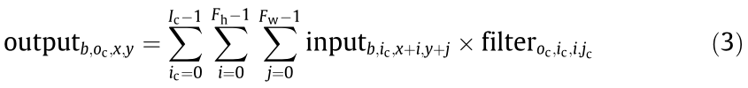
where Fh is the height of the filter, Fw is the width of the filter, i is the index of the row in a 2D filter, j is the index of the column in a 2D filter, x is the index of the row in a 2D feature map, y is the index of the column in a 2D feature map. For 0 ≤ b < B, 0 ≤oc < Oc, 0 ≤ x < Oh, 0 ≤ y < Ow (Oh: the height of the output feature map; Ow: the width of the output feature map).
《Fig. 2》
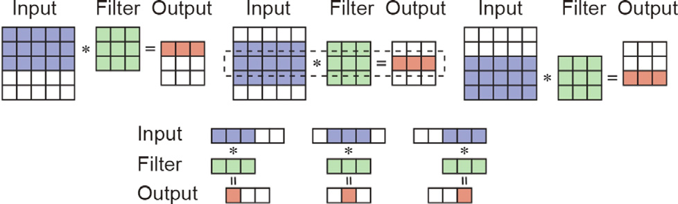
Fig. 2. Two levels of sliding windows in 2D convolution [26]. *: convolution.
To provide translation invariance, the same convolutional filter is repeatedly applied to all the parts of the input feature map, making the data reuse pattern in convolutions much more complex than in matrix multiplications. For easier hardware implementation, it is better to view the 2D sliding window in a two-level hierarchy: The first level is a window of several rows that slides downward to provide inter-row data reuse, and the second level is a window of several elements that slides rightward to provide intra-row data reuse.
Although the computation patterns of matrix multiplications and convolutions are very different, they can actually be converted to each other. Thus, an accelerator designed for one type of computation can still support the other type, although doing so might not be very efficient. Convolutions can be transformed into matrix multiplication through the Toeplitz matrix, as illustrated in Fig. 3, at the cost of introducing redundant data. On the other hand, matrix multiplication is just a convolution with Oh = Ow = Fw = Fh = 1. The feature map and the filter are reduced to a single element.
《Fig. 3》
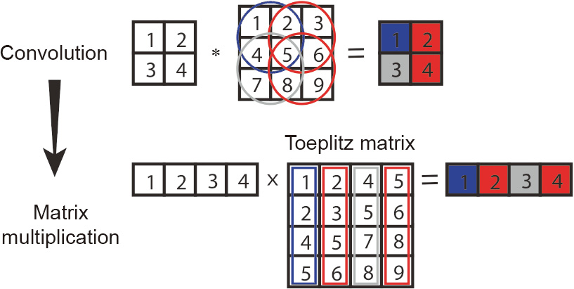
Fig. 3. Converting convolution to Toeplitz matrix multiplication. *: convolution.
《2.3. Resistive memory》
2.3. Resistive memory
The memristor, also known as the ReRAM, is an emerging nonvolatile memory that stores information using cell resistances. In 2008, HP Lab reported its discovery of a nanoscale memristor based on TiO2 thin-film devices [27]. Since then, many resistive materials and structures have been found or rediscovered.
As demonstrated in Fig. 4(a), each ReRAM cell has a metal-oxide layer sandwiched between a top electrode (TE) and a bottom electrode (BE). The resistance of a memristor cell can be programmed by applying a current or voltage with an appropriate pulse width or magnitude. In particular, the data stored in a cell can be represented by the resistance level accordingly: A low resistance state (LRS) denotes bit ‘‘1,” while a high resistance state (HRS) denotes bit ‘‘0.” For a read operation, a small sensing voltage is applied across the device; the amplitude of the current is then determined by the resistance.
In 2012, HP Lab proposed a ReRAM crossbar structure that has demonstrated an attractive capability to efficiently accelerate matrix–vector multiplications in NNs. As shown in Fig. 4(b), the vector is represented by the input signals on the wordlines (WLs). Each element of the matrix is programmed into the conductance of a cell in the crossbar array. Thus, the current summing at the end of each bitline (BL) is viewed as the result of the matrix– vector multiplication. For a large matrix that cannot fit in a single array, the input and the output are partitioned and grouped into multiple arrays. The output of each array is a partial sum, which is collected horizontally and summed vertically to generate the actual results.
《Fig. 4》

Fig. 4. The ReRAM basics. (a) ReRAM cell; (b) 2D ReRAM crossbar. V : write voltage; Vr : read voltage; BL: bitline; WL: wordline; TE: top electrode; BE: bottom electrode; LRS: low resistance state; HRS: high resistance state.
《3. On-chip accelerators》
3. On-chip accelerators
In the early stage of DNN accelerator design, accelerators were designed for the acceleration of approximate programs in generalpurpose processing [28], or for small NNs [13]. Although the functionality and performance of on-chip accelerators were very limited, they revealed the basic idea of AI-specialized chips. Because of the limitations of general-purpose processing chips, it is often necessary to design specialized chips for AI/DNN applications.
《3.1. The neural processing unit》
3.1. The neural processing unit
The neural processing unit (NPU) [28] is designed to use hardwarelized on-chip NNs to accelerate a segment of a program instead of running on a central processing unit (CPU).
The hardware design of the NPU is quite simple. An NPU consists of eight processing engines (PEs), as shown in Fig. 5. Each PE performs the computation of a neuron; that is, multiplication, accumulation, and sigmoid. Thus, what the NPU performs is the computation of a multiple layer perceptron (MLP) NN.
《Fig. 5》
Fig. 5. The NPU [28]. (a) Eight-PE NPU; (b) single PE. FIFO: first in, first out.
The idea of using the hardwarelized MLP—that is, the NPU—to accelerate some program segments was very inspiring. If a program segment is ① frequently executed and ② approximable, and if ③ the inputs and outputs are well defined, then that segment can be accelerated by the NPU. To execute a program on the NPU, programmers need to manually annotate a program segment that satisfies the above three conditions. Next, the compiler will compile the program segment into NPU instructions and the computation tasks are offloaded from the CPU to the NPU at runtime. Sobel edge detection and fast fourier transform (FFT) are two examples of such program segments. An NPU can reduce up to 97% of the dynamic CPU instructions and achieve a speedup of up to 11.1 times.
《3.2. RENO: A reconfigurable NoC accelerator》
3.2. RENO: A reconfigurable NoC accelerator
Unlike the NPU, which is designed for the acceleration of generalpurpose programs, RENO [13] is an accelerator for NNs. RENO uses a similar idea for the PE design, as shown in Fig. 6. However, the PE of RENO is based on ReRAM: RENO utilizes the ReRAM crossbar as the basic computation unit to perform matrix–vector multiplications. Each PE consists of four ReRAM crossbars, which respectively correspond to the processing of positive and negative inputs and positive and negative weights. In RENO, routers are deployed to coordinate data transfer between the PEs. Unlike conventional CMOS routers, the routers of RENO transfer the analog intermediate computation results from the previous neuron to the following neuron. In RENO, only the input and final output are digital; the intermediate results are all analog and are coordinated by the analog routers. Data converters (DACs and ADCs) are required only when transferring data between RENO and the CPU.
《Fig. 6》
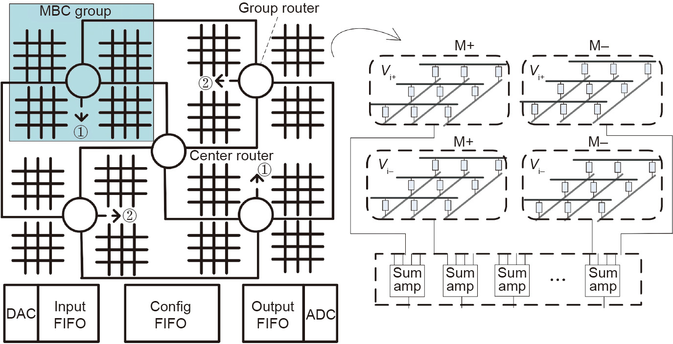
Fig. 6. RENO architecture [13]. MBC: memristor-based crossbars; Vi+: positive input voltage; Vi–: negative input voltage; M+: the MBC mapped with positive weights; M–: the MBC mapped with negative weights; Sum amp: summation amplifier.
RENO supports the processing of the MLP and the autoassociate memory (AAM), and corresponding instructions are designed for the pipelining of RENO and a CPU. Because RENO is an on-chip design, the supported applications are limited. RENO supports the processing of small datasets, such as the UCI ML repository [29] and the tailored Modified National Institute of Standards and Technology (MNIST) database [30].
《4. Stand-alone DNN/convolutional neural network accelerator》
4. Stand-alone DNN/convolutional neural network accelerator
For broadly used DNN and convolutional neural network (CNN) applications, stand-alone domain-specific accelerators have achieved great success in both cloud and edge scenarios. Compared with general-purpose CPUs and graphics processing units (GPUs), these custom architectures offer better performance and higher energy efficiency. Custom architectures usually require a deep understanding of the target workloads. The dataflow (or data reuse pattern) is carefully analyzed and utilized in the design to reduce the off-chip memory access and improve the system efficiency.
In this section, we respectively use the DianNao series [31] and the tensor processing unit (TPU) [5] as academic and industrial examples to explain stand-alone accelerator designs and discuss the dataflow analysis.
《4.1. The DianNao series: An academic example》
4.1. The DianNao series: An academic example
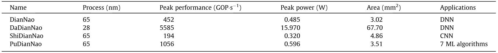
The DianNao series includes multiple accelerators, listed in Table 1 [31]. DianNao is the first design of the series. It is composed of the following components, as shown in Fig. 7:
《Table 1》
Table 1 DianNao series accelerators [31].
GOP: group of picture.
《Fig. 7》
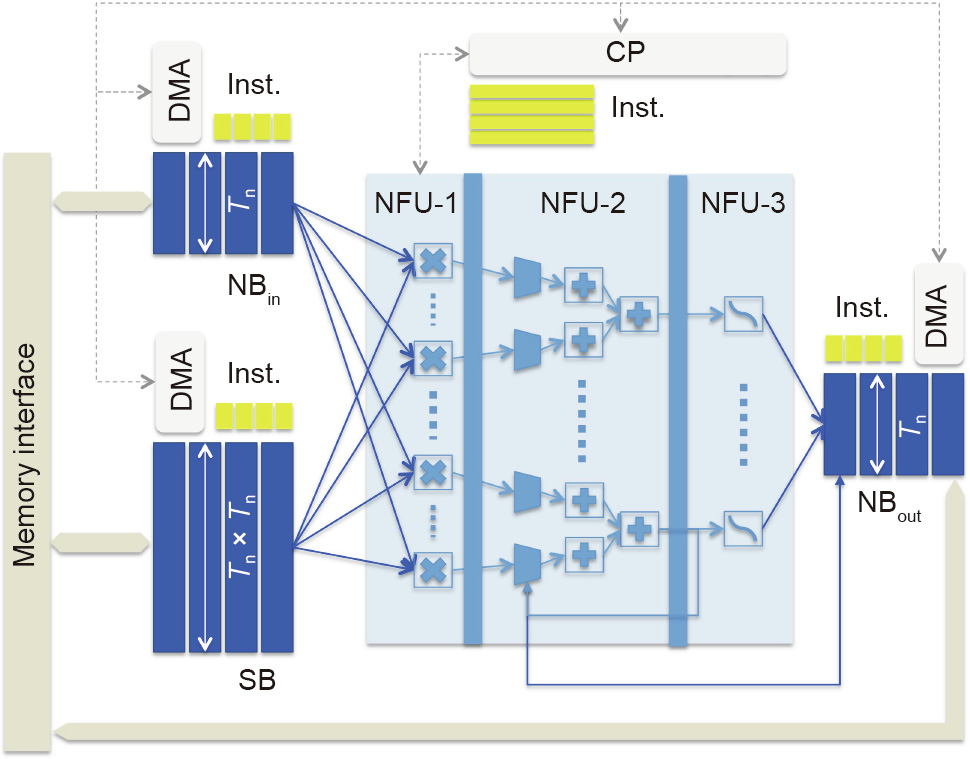
Fig. 7. The DianNao architecture [18]. DMA: direct memory access; Inst.: instructions; Tn: the number of output neurons.
(1) A computational block neural functional unit (NFU), which performs computations;
(2) An input buffer for input neurons (NBin);
(3) An output buffer for output neurons (NBout);
(4) A synapse buffer for synaptic weights (SB);
(5) A control processor (CP).
The NFU, which includes multipliers, adder trees, and nonlinear functional units, is designed as a pipeline. Rather than a normal cache, a scratchpad memory is used as on-chip storage because it can be controlled by the compiler and can easily explore the data locality.
While efficient computing units are important for a DNN accelerator, inefficient memory transfers can also affect the system throughput and energy efficiency. The DianNao series introduces a special design to minimize memory transfer latency and enhance system efficiency. DaDianNao [16] targets the datacenter scenario and integrates a large on-chip embedded dynamic random access memory (eDRAM) to avoid a long main-memory access time. The same principle applies to the embedded scenario. ShiDianNao [19] is a DNN accelerator dedicated to CNN applications. Because of weight sharing, a CNN’s memory footprint is much smaller than that of other DNNs. It is possible to map all of the CNN parameters onto a small on-chip static random access memory (SRAM) when the CNN model is small. In this way, ShiDianNao avoids expensive off-chip dynamic random access memory (DRAM) access and achieves a 60 times energy efficiency in comparison with DianNao.
PuDianNao [17] is designed for multiple ML applications. In addition to supporting DNNs, it supports other representative ML algorithms, such as k-means and classification trees. To deal with the different data-access patterns of these workloads, PuDianNao introduces a cold buffer and a hot buffer for data with different reuse distances in its architecture. Moreover, compilation techniques, including loop unrolling, loop tiling, and cache blocking, are introduced as a software-and-hardware co-design method to increase the on-chip data reuse and the PE utilization ratios.
On top of the stand-alone accelerators, a domain-specific instruction set architecture (ISA), called Cambricon [32], was proposed to support a broad range of NN applications. Cambricon is a load-store architecture that integrates scalar, vector, matrix, logical, data transfer, and control instructions. The ISA design considers data parallelism, customized vector/matrix instructions, and the use of scratchpad memory.
The successors of the Cambricon series introduce support to sparse NNs. Other accelerators support more complicated NN workloads, such as long short-term memory (LSTM) and generative adversarial network (GAN). These works will be discussed in detail in Section 6.
《4.2. The TPU: An industrial example》
4.2. The TPU: An industrial example
Highlighted with a systolic array, as shown in Fig. 8, google published its first tpu paper (tpu1) in 2017 [5]. tpu1 focuses on inference tasks, and has been deployed in google’s datacenter since 2015. the structure of the systolic array can be regarded as a specialized weight-stationary dataflow, or a 2d single instruction multiple data (simd) architecture.ed with a systolic array, as shown in Fig. 8, Google published its first TPU paper (TPU1) in 2017 [5]. TPU1 focuses on inference tasks, and has been deployed in Google’s datacenter since 2015. The structure of the systolic array can be regarded as a specialized weight-stationary dataflow, or a 2D single instruction multiple data (SIMD) architecture.
《Fig. 8》
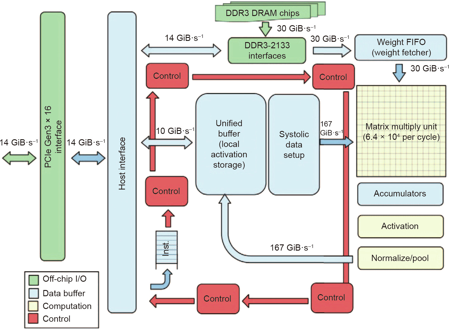
Fig. 8. TPU block diagram [5]. DDR3: double-data-rate 3; PCle: Peripheral Component Interconnect Express.
After that, in Google I/O’17 [33], Google announced its cloud TPU (also known as TPU2), which can handle both training and inference in the datacenter. TPU2 also adopts a systolic array and introduces vector-processing units. In Google I/O’18 [34], Google announced TPU3, which is highlighted as having liquid cooling. In Google Cloud Next’18 [35], Google announced its edge TPU, which targets the inference tasks of the Internet of Things (IoT).
《4.3. Dataflow analysis and architecture design》
4.3. Dataflow analysis and architecture design
A DNN/CNN generally requires a large memory footprint. For large and complicated DNN/CNN models, it is unlikely that the whole model can be mapped onto the chip. Due to the limited off-chip bandwidth, it is of vital importance to increase on-chip data reuse and reduce the off-chip data transfer in order to improve the computing efficiency. During architecture design, dataflow analysis is performed and special consideration needs to be taken. As shown in Fig. 9 [15,36], Eyeriss explored different NN dataflows, including input-stationary (IS), output-stationary (OS), weight-stationary (WS), and no-local-reuse (NLR) dataflows, in the context of a spatial architecture and proposed the rowstationary (RS) dataflow to enhance data reuse.
《Fig. 9》
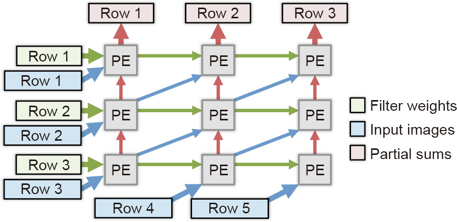
Fig. 9. Row-stationary dataflow [15,36].
The high-efficient dataflow design inspired many practical designs in the AI chip industry. For example, WaveComputing features a coarse-grained reconfigurable array (CGRA)-based dataflow processor [37]. GraphCore focuses on graph architecture and is claimed to be able to achieve higher performance than the traditional scalar processor and vector processor on AI workloads [38].
《5. Accelerators with emerging memories》
5. Accelerators with emerging memories
ReRAM [27] and the hybrid memory cube (HMC) [39] are representative emerging memory technologies and memory structures that enable processing-in-memory (PIM). PIM can greatly reduce the data movements in computing platforms, as the data movement between CPUs and off-chip memory consumes two orders of magnitude more energy than a floating point operation [40]. DNN accelerators can take these benefits from ReRAM and HMC and apply PIM to accelerate DNN executions.
《5.1. ReRAM-based DNN accelerators》
5.1. ReRAM-based DNN accelerators
The key idea of utilizing ReRAM for DNN acceleration is to use the ReRAM array as a computation engine for matrix–vector multiplications [41,42], as mentioned in Section 2.3. PRIME [21], ISAAC [25], and PipeLayer [22] are three representative ReRAM-based DNN accelerators.
The architecture of PRIME [21] is shown in Fig. 10. PRIME revises the ReRAM for both data storage and computation. In PRIME, the wordline decoders and drivers are configured with multilevel voltage sources, so the input feature map can be applied to the memory array in computation. The column multiplexer is configured with analog subtraction and sigmoid circuitry; thus, partial results from two arrays are combined and sent to the nonlinear activation (sigmoid). The sense amplifier is also reconfigurable in sensing resolution, and performs the functionality of an ADC.
《Fig. 10》
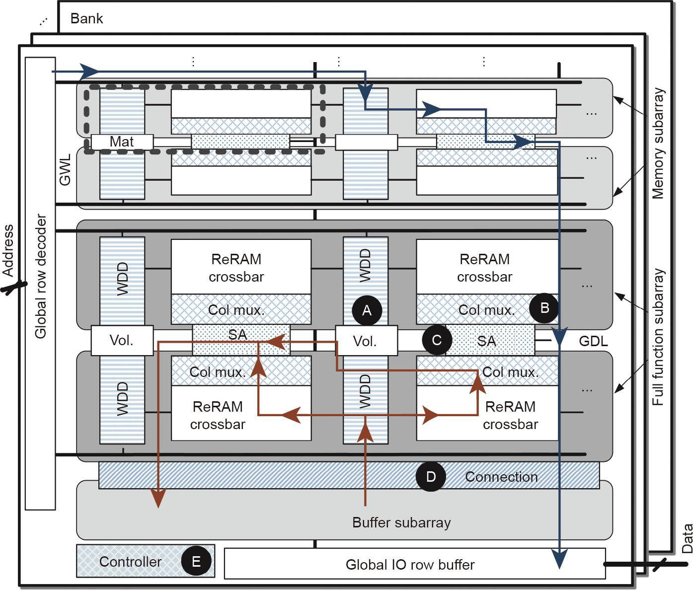
Fig. 10. PRIME architecture [21]. GWL: global word line; SA: sense amplifier; WDD: wordline decoder and driver; GDL: global data line; IO: input and output; Vol.: voltage source; Col mux.: column multiplexer.
ISAAC [25] proposes an intra-tile pipeline design for NN processing in ReRAM, as shown in Fig. 11. The pipeline design combines data encoding and computation. IMA is the ReRAM-based in situ multiply accumulate unit. In the pipeline, in the first cycle, data is fetched from eDRAM to the computation tile. The data format in ISAAC is fixed 16 bit. In computation, in each cycle, 1 bit is input to the IMA, and the computation result from the IMA is converted to digital format, shifted by 1 bit, and accumulated. Therefore, it takes another 16 cycles to process the input. The nonlinear activation is then applied, and the results are written back to eDRAM.
《Fig. 11》
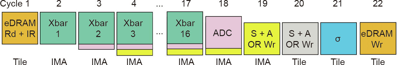
Fig. 11. Intra-tile pipeline in ISAAC [25]. Rd: read; IR: input register; Xbar: crossbar; S + A: shift and add; OR: output register; Wr: write; σ : sigmoid unit; IMA: the ReRAMbased in situ multiply accumulate unit.
Tiled computation architecture is a natural and widely used way to process NNs. It is necessary to explore coarse-grained parallel designs to improve the accelerators’ throughput. PipeLayer [22] introduces intra-layer parallelism and an inter-layer pipeline for tiled architecture, as illustrated earlier in Fig. 1. For intralayer parallelism, PipeLayer uses a data-parallel scheme, which duplicates processing units with the same weights to process multiple data in parallel. For the inter-layer pipeline, buffers are delicately employed for data sharing between weighted layers. As a result, the processing of layers from multiple data can be parallelized. The inter-layer pipeline is a model parallel scheme.
《5.2. HMC-based DNN accelerators》
5.2. HMC-based DNN accelerators
An HMC vertically integrates DRAM dies and the logic die. The high memory capacity, high memory bandwidth, and low latency offered by an HMC enables near-data processing. In an HMCbased accelerator design, computation and logic units are placed on the logic die, and the DRAM dies in a vault are used for data storage. Neurocube [43] and Tetris [44] are two DNN accelerators based on an HMC.
A whole accelerator in Neurocube has one HMC with 16 vaults [43]. As shown in Fig. 12, each vault can be viewed as a subsystem, which consists of a PE to perform multiply-accumulation (MAC) and a router for package transferring between the logic die and the dies of DRAM. Each vault can send data to a destination vault by the router, which enables out-of-order data arrival. For each PE, if the buffer (16 entries) is filled with data, the computation will start.
《Fig. 12》

Fig. 12. Neurocube architecture and PE design [43]. VC: vault controller; PNG: programmable neurosequence generator; TSV: through silicon via; A, B, C: input operands; Y: output operand; R: register; μ: microcontroller.
Tetris [44] also employs 16 PEs in one HMC, but it uses a spatial mesh to connect the PEs. Tetris proposes a bypassing ordering scheme, which is similar to the data stationary scheme discussed in Refs. [15,36], to improve data reuse. To minimize data remote access, Tetris explores the partitioning of input and output feature maps.
《6. Accelerators for emerging applications》
6. Accelerators for emerging applications
The efficiency of DNN accelerators can be also improved by applying efficient NN structures. NN pruning, for example, makes the model small yet sparse, thus reducing the off-chip memory access. The NN quantization allows the model to operate in a low-precision mode, thus reducing the required storage capacity and computational cost. Emerging applications, such as the GAN and the RNN, raise special requirements for dedicated accelerator designs. This section discusses accelerator designs for the sparse NN, low precision NN, GAN, and RNN.
《6.1. Sparse neural network》
6.1. Sparse neural network
Previous work in dense-sparse-dense (DSD) [46] has shown that a large proportion of NN connections can be pruned to zero with or without minimum accuracy loss. Many corresponding computing architectures have also been proposed. For example, EIE [47] and Cnvlutin [48] respectively target accelerating the computations of NN models with sparse weight matrices and sparse feature maps. However, the special data format and extra encoder/decoder adopted in these designs introduce additional hardware cost. Some algorithm works discuss how to design NN models in a hardwarefriendly way, such as by using block sparsity, as shown in Fig. 13 [45]. Techniques that can handle irregular memory access and an unbalanced workload in sparse NN have also been proposed. For example, Cambricon-X [49] and Cambricon-S [50] address the memory access irregularity in sparse NNs through a cooperative software/hardware approach. ReCom [51] proposes a ReRAMbased sparse NN accelerator based on structural weight/activation compression.
《Fig. 13》

Fig. 13. Structural sparsity: filter-wise, channel-wise, shape-wise, and depth-wise sparsity, as shown in Ref. [45]. W : DNN weights; l : the index of weight tensor; cl : output channel length; nl : input channel length; ml : kernel height; kl : kernel width; ": " is a placeholder.
《6.2. Low precision neural network》
6.2. Low precision neural network
Reducing data precision or quantization, is another viable way to improve the computing efficiency of DNN accelerators. The recent TensorRT results [52] show that the widely used NN models, including AlexNet, VGG, and ResNet, can be quantized to 8 bit without inference accuracy loss. However, it is difficult for such a unified quantization strategy to retain the network’s accuracy when further lower precision is adopted. Many complex quantization schemes have been proposed, however, significantly increasing the hardware overhead of the quantization encoder/decoder and the workload scheduler in the accelerator design. As shown in the following discussion, a “sweet point” exists between data precision and overall system efficiency with various optimizations.
(1) The weight and feature map are quantized into different precisions to achieve lower inference accuracy loss. This may change the original dataflow and affect the accelerator architecture, especially the scratchpad memory.
(2) Different layers or different data may require different quantization strategies. In general, the first and the last layer of the NN require higher precision. This fact increases the design complexity of the quantization encoder/decoder and the workload scheduler.
(3) New quantization schemes have been proposed by observing the characteristics of the data distribution. For example, an outlier-aware accelerator [53] performs dense and low-precision computations for a majority of data (weights and activations) while efficiently handling a small number of sparse and highprecision outliers.
(4) A new data format has been proposed to better represent low-precision data. For example, the compensated DNN [54] introduces a new fixed-point representation: fixed point with error compensation (FPEC). This representation has two parts: ① computation bits, which are the conventional fixed-point format; and ② compensation bits, which represent the quantization error. This work also proposes a low-overhead sparse compensation scheme to estimate the error in the MAC design.
《6.3. Generative adversarial network》
6.3. Generative adversarial network
Compared with the original DNN/CNN, the GAN consists of two NNs: namely, the generator and the discriminator. The generator learns to produce fake data, which is supplied to the discriminator, and the discriminator learns to distinguish the generated fake data. The goal is to have the generator generate fake data that eventually cannot be differentiated by the discriminator. These two NNs are trained iteratively and compete with each other in a minimax game. The GAN’s operations involve a new operator, called transposed convolution (also known as deconvolution or fractionally strided convolution). Compared with the original convolution, transposed convolution performs up-sampling with a lot of zeros inserted into the feature maps. Redundant computation will be introduced if the transposed convolution is mapped straightforwardly. Techniques are also needed to deal with nonstructural memory access and irregular data layout if zeros are bypassed. In summary, compared with the stand-alone DNN/CNN inference accelerators discussed in Section 4, GAN accelerators must ① support training, ② accommodate transposed convolution, and ③ optimize the nonstructural data access.
ReGAN proposes a ReRAM-based PIM GAN architecture [23]. As shown in Fig. 14, a dedicated pipeline is designed for layer-wise computation in order to increase the system throughput. Two techniques, called spatial parallelism and computation sharing, are proposed to further improve training efficiency. LerGAN [55] proposes a zero-free data-reshaping scheme to remove the zero-related computation in ReRAM-based PIM GAN architecture. A reconfigurable interconnection scheme is proposed to reduce the data transfer overhead.
《Fig. 14》
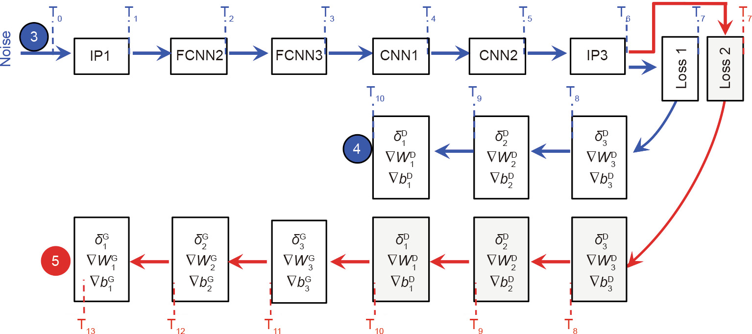
Fig. 14. Computation sharing pipeline in ReGAN [23]. T: logical cycle;  : error map of discriminator;
  : error map of generator;
  : partial derivative of the weights in discriminator;
  : partial derivative of the weights in generator;
  : partial derivative of the bias in discriminator;
  : partial derivative of the bias in generator; IP: input project layer; FCNN: fractional-strided convolution layer.
For a CMOS-based GAN accelerator, previous work [56] proposed efficient dataflow for different steps in a GAN; that is, zero-free output stationary (ZFOST) for feed-forward/backward propagation, and zero-free weight stationary (ZFWST) for the weight update. GANAX [57] proposed a unified SIMD-multiple instruction multiple data (MIMD) accelerator to maximize the efficiency of both the generator and the discriminator: The SIMD-MIMD mode is used in selective executions due to the zero insertion in the generator, while the pure SIMD mode is used to operate the conventional CNN in the discriminator.
《6.4. Recurrent neural network》
6.4. Recurrent neural network
The RNN has many variants, including gated recurrent units (GRU) and LSTM. The recurrent property of the RNN leads to complicated data dependency, in comparison with the conventional DNN/CNN.
ESE [58] demonstrated an accelerator dedicated to sparse LSTM. A load-balance-aware pruning is proposed to ensure high hardware utilization. A scheduler is designed to encode and partition the compressed model to multiple PEs for parallelism and schedule the LSTM dataflow. DNPU [59] presented an 8.1TOPS/W reconfigurable CNN-RNN system-on-chip (SoC) DeltaRNN [60] leveraged the RNN delta network update approach to reduce memory access: The output of a neuron updates only when the neuron’s activation changes by more than a delta threshold.
《7. The future of DNN accelerators》
7. The future of DNN accelerators
In this section, we share our perspectives about the future of DNN accelerators. We discuss three possible future trends: ① DNN training and accelerator arrays, ② ReRAM-based PIM accelerators, and ③ DNN accelerators on edge devices.
《7.1. DNN training and accelerator arrays》
7.1. DNN training and accelerator arrays
Currently, almost all DNN accelerator architectures focus on optimization for DNN inference within the accelerator itself, and very few considered the training support [22]. The presumption is that the DNN model has already been trained before deployment. Very few accelerator architectures exist that can support DNN training. Following the increase of the size of training datasets and NNs, a single accelerator is no longer capable of supporting the training of a large DNN. It is inevitably necessary to deploy an array of accelerators or multiple accelerators for the training of DNNs.
A hybrid parallel structure for DNN training on an accelerator array is proposed in Ref. [61]. The communication between the accelerators dominates the time and energy consumption in DNN training on an accelerator array. Ref. [61] proposes a communication model to identify where the data communication is generated and how large the traffic is. Based on the communication model, layer-wise parallelism is optimized to minimize the total communication and improve the system performance and energy efficiency.
《7.2. ReRAM-based PIM accelerator for DNNs》
7.2. ReRAM-based PIM accelerator for DNNs
Current ReRAM-based accelerators, such as those described in Refs. [21,22,25,62], assume ideal memristor cells. However, realistic challenges such as process variation [63,64], circuit noise [65,66], retention issues, and endurance issues [67–69] greatly hinder the realization of ReRAM-based accelerators. There are also very few silicon proofs of ReRAM-based accelerators and advanced architectures such as PIM, except for that provided in Ref. [70]. In practical ReRAM-based DNN accelerator designs, these non-ideal factors must be taken into consideration.
《7.3. DNN accelerators on edge devices》
7.3. DNN accelerators on edge devices
In edge-cloud DNN applications, the computational and memory-intensive parts (e.g., training) are often offloaded onto the powerful GPUs in the cloud, and only certain light inference models are deployed on edge devices (e.g., the IoT or mobile devices).
Following the rapid increase in data acquisition scale, it has become desirable to have intelligent edge devices that are capable of adaptively learning or fine-tuning their DNN models for certain tasks. For example, in wearable applications that monitor the health of users, it will be helpful to adapt the CNN models locally rather than sending the sensed health data back to the cloud, due to significant data communication overhead and privacy issues. In other applications, such as robots, drones, and autonomous vehicles, statically trained models cannot efficiently handle the time-varying environmental conditions.
However, the long data-transmission latency of sending huge amounts of environmental data to the cloud for incremental training is often unacceptable. More importantly, many real-life scenarios require real-time execution of multiple tasks and dynamic adaptation capability [58]. Nevertheless, it is extremely challenging to perform learning in edge devices because of their stringent computing resources and tight power budget. RedEye [71] is an accelerator for DNN processing on the edge, where the computation is integrated with sensing. Designing lightweight, real-time, and energy-efficient architectures for DNNs on the edge is an important research direction to pursue next.
《Acknowledgements》
Acknowledgements
This work was supported in part by the National Science Foundations (NSFs) (1822085, 1725456, 1816833, 1500848, 1719160, and 1725447), the NSF Computing and Communication Foundations (1740352), the Nanoelectronics COmputing REsearch Program in the Semiconductor Research Corporation (NC-2766- A), the Center for Research in Intelligent Storage and Processing-in-Memory, one of six centers in the Joint University Microelectronics Program, a SRC program sponsored by Defense Advanced Research Projects Agency.
《Compliance with ethics guidelines》
Compliance with ethics guidelines
Yiran Chen, Yuan Xie, Linghao Song, Fan Chen, and Tianqi Tang declare that they have no conflicts of interest or financial conflicts to disclose.


 京公网安备 11010502051620号


