
《1. Introduction》
1. Introduction
Manufacturing of extremely small size (down to nanoscale) patterns with the lowest possible cost is an unremitting pursuit for large data storage, high-speed computation, and low power consumption in the semiconductor industry. Owing to the intrinsic diffraction limit of the optical system, the extreme ultraviolet (EUV) lithography technique with extreme small wavelength is proposed to further push the nanofabrication limit [1,2]. However, the high cost and extreme complexity of the state-of-art lithography tool in the semiconductor industry seriously hinder the applications in small volume and high-freedom nanofabrication that is essential for fundamental research and nano-devices prototyping. Maskless lithography, such as electron beam lithography (EBL) [3,4], focused ion beam (FIB) lithography [5,6], scanning-probe lithography (SPL) [7], and direct laser writing (DLW) [8] provides alternative methods for flexible nanofabrication. However, the low throughput and high cost of EBL and FIB limit their application only in template fabrication and special sample preparation. SPL is a probe-based, low cost scheme operated in an ambient environment, but the throughput is still difficult to increase because of its limited bandwidth to active control the probe–substrate distance at a high scanning speed. DLW, especially ultrafast laser processing, can achieve high 0.1–1 μm resolution and processing speeds approximately meters-per-second, while it is still restricted by the optical diffraction limit.
Lithography in the near-field range, using surface plasmon polariton (SPP) and plasmonic nanolithography (PNL) to generate sub-diffraction-limited nanostructures, has been developed to overcome these obstacles [9–14]. It offers a possibility to break through the diffraction limit and achieve high-resolution nanofabrication with a light source from ultraviolet (UV) to infrared (IR) in an ambient environment. Fig. 1(a) shows the comparison between currently realized PNL and the various nanofabrication technologies in terms of resolution, throughput, and cost. The PNL system can significantly improve the throughput under atmospheric environments compared to the conventional maskless lithography with high resolution and ultra-low cost. In PNL, a plasmonic lens (PL) is a key element to generate a sub-diffraction-limited light spot with especially designed plasmonic nanostructures. To ensure the coupling power into the photoresist and the uniformity of the linewidth, the gap between the PL and photoresist should be precisely maintained in the near field less than tens of nanometers in the range of the SPP decay distance. Therefore, static contact PNL has been first demonstrated to achieve the processing of subdiffraction-limited structures. To further improve the throughput and freedom of this technique, three types of direct-writing systems were studied based on different strategies of gap control: contact mode (CM) [14–17], active control mode (ACM) [18–20], and passive control mode (PCM) [21–24]. In CM, a contact probe with lubricant layer is used, which results in low scan speed and possible damage to the photoresist. ACM has a gap feedback system to control the distance, leading to the limited bandwidth available to achieve high-speed lithography and high requirements for environmental vibration and noise control. In a PCM system, a plasmonic flying head (PFH) with PL on it supported by a high stiffness air film can realize high-speed and high-bandwidth nanofabrication, which is a more attractive technology for plasmonic lithography. Srituravanich et al. [22] first proposed the concept of plasmonic lithography using PCM. However, the relatively large PL–photoresist gap and the design of the PL resulted in 80 nm linewidth fabrication. With multistage PL design coupling of the propagating surface plasmon (PSP) and localized surface plasmon (LSP), a smaller linewidth of 22 nm half-pitch with pulsed lasers was also achieved. However, a smaller light spot size has not been achieved with continuous lasers, and the PL is polarization sensitive, which poses a challenge for practical alignment. Therefore, a smaller and steadier gap should be explored by a more systematic flying head design, and a new scheme of PL for any polarizations of light source is also needed to achieve a smaller size and stable nanofabrication. Furthermore, more efficient processing can be achieved by parallel fabrication.
《Fig. 1》

Fig. 1. Schematic of the parallel plasmonic direct-writing nanolithography (PPNL) system. (a) Nanofabrication landscape: resolution, cost, and throughput of different nanofabrication methods. PNL is a good high-resolution fabrication method for relatively high throughput at low cost. GEB: Gaussian electron beam lithography; VSB: variable shaped electron beam lithography; DUV: deep ultraviolet; NIL: nanoimprint lithography. (b) The proposed PPNL system. A laser beam with a controllable polarization shine on the plasmonic flying head (PFH) with the plasmonic lens array (PLA) to generate SPP in the near-field range. With controlling of substrate rotation and the nano-precision translation stage, the PFH can expose the photoresist with desired patterns. (c) The PFH with a designed air bearing surface (ABS) topography that has three degrees of freedom (DOFs) (flying-height (FH), pitch angle, and roll angle), flies at tens of nanometers on the high-speed rotating photoresist-coated substrate to provide a near-field condition. (d) The designed ABS topography on the PFH slider. (e) Metasurface-based plasmonic lens (PL) array on the minimum FH (MFH) location.
Herein, we establish and experimentally demonstrate a parallel plasmonic direct-writing nanolithography (PPNL) system. A novel air bearing surface (ABS) of PFH is systematically designed by considering the static (flying-height (FH) and its uniformity), dynamic (stiffness and shock performance), and load/unload performance with an in-house developed simulator to achieve uniform around 15 nm minimum FH (MFH) and around 63 microradian (μrad) pitch angle at a range of 8–18m·s–1 . A multi-stage polarization insensitive metasurface-cylinder PL combining the PSP and LSP is proposed to couple more power and realize a more confined spot. With such key components, parallel lithography of nanostructures with the smallest around 26 nm linewidth is achieved with the prototyping system. Moreover, the system can be further miniaturized to the size of the mobile hard disk drive (HDD), which holds a great potential for high-freedom and low-cost nanofabrication.
《2. Material and methods》
2. Material and methods
《2.1. Numerical simulation》
2.1. Numerical simulation
The numerical simulation of PFH is calculated by the in-house developed solver based on COMSOL 4.2 (COMSOL, Sweden) [25]. A six degrees of freedom (DOFs) model of the PFH is established to calculate the static, dynamic, and load/unload process. The model divides the suspension into three parts, namely, the tab, local suspension, and main suspension, as shown in Fig. S1 in Appendix A. The interaction between the suspension and head consists of three parts: the dimple/head contact force, gimbal force/ moments, and limiter contact force. The head has three DOFs with corresponding posture parameters of FH, pitch angle, and roll angle. The aerodynamics force, head/substrate contact force, and intermolecular force act on the head/substrate interface (HSI). The key of the passive flight of the PFH is the aerodynamics force that can be calculated by the rarefied gas Reynolds equation:

where P is dimensionless pressure p/p0; p and p0 are the air bearing pressure and ambient pressure, respectively; H is the dimensionless air bearing thickness;  is the bearing number defined as
  , μ is the ambient gas viscosity, U is the dimensionless gas velocity, L is dimensionless length of the head, h0 is reference thickness of the air bearing; ψ is the squeeze number defined as
  ,
,  is the angular velocity; T is dimensionless time; and Q is a modification coefficient to account for gaseous rarefaction effects with Fukui and Kaneko’s model [26]. With this model, the static, dynamic, and load/unload performance is analyzed as shown in Figs. S2–S7 in Appendix A.
The numerical simulation of PL is calculated by the finitedifference time-domain (FDTD) software (FDTD Solutions, Lumerical Inc., Canada). The perfectly matched layer is employed for the horizontal (X and Y) directions and the vertical (Z) direction in the simulation. The refractive index of chromium and platinum are obtained from Ref. [27].
《2.2. PFH fabrication and assembly》
2.2. PFH fabrication and assembly
A 2 in (1 in = 2.54 cm) quartz substrate is prepared with a thickness of 200 μm, which is the initial thickness of the PFH slider. Subsequently, a BP212-37 UV positive resist is spin coated on the substrate and baked in an oven at 100 °C for 5 min to completely remove the photoresist solvent. The sample is exposed in an exposure dose of 62 mJ·cm–2 in a lithography machine for an exposure time of 70 s with the deepest mask of the ABS structure that has a mark on it. Development is then carried out with a 0.5% aqueous solution of sodium hydroxide (NaOH) for 20 s. Subsequently, a chromium (Cr) film is sputtered in the sputtering station under the radio frequency (RF) power of 50W to a thickness of around 100 nm and then lifted off with acetone. The quartz substrate is then etched by the reactive ion etching (RIE) method under the reaction gas of trifluoromethane (CHF3) and the RF power of 300W to 2.6 μm depth. The Cr film is removed using cerium ammonium nitrate. The sample is then exposed twice with alignment in the same way using two other masks with etching depths of 0.7 and 0.1 μm. The mask design is provided in Fig. S8 in Appendix A. The diamond dicing machine is then used to slice the substrate to sliders.
An in-house developed dual charge-coupled device (CCD) system is used to assemble the slider on the commercial suspension as shown in Fig. S9 in Appendix A. During assembly, the dimple on the suspension should coincide to the geometric center of the slider with the alignment of the upper and lower CCDs because the suspension exerts only longitudinal forces on the slider without pitch or roll moments. Here, the UV curable adhesive is used to bond the flying head slider to the suspension.
《2.3. PL fabrication》
2.3. PL fabrication
The fabrication of PL is performed using the FIB/scanning electron microscopy (SEM) dual beam system (TESCAN LYRA 3, TESCAN, Czech Republic), and a layer of 60 nm Cr is first sputtered on the ABS before processing. For a bowtie-shape array, due to the small structure, the beam current is 1 pA, and the beam spot diameter is 5 nm. The array period is 500 nm. For the multi-stage PL array (PLA), the metasurface is first etched by a beam of 10 pA, and then the cylinder is induced deposition by platinum with a beam of 1 pA.
《2.4. Tellurium oxide (TeOx) film sputtering, analysis, and lubricant coating》
2.4. Tellurium oxide (TeOx) film sputtering, analysis, and lubricant coating
The magnetron sputtering coating machine (MSP-300B, Beijing Chuangshiweina Technology Co., Ltd., China) is used to prepare TeOx, where x represents the oxygen content in tellurium (Te) oxide. A metal elemental Te is used as a target, and the RF power supply is 50W. The ratio of oxygen (O) to argon (Ar) in the chamber is adjusted to achieve reactive sputtering and different values of x. An experimental study of the film components using X-ray photoelectron spectroscopy (XPS) is performed to obtain a suitable oxygen-to-argon ratio.
A perfluoropolyether (PFPE) lubricant is widely used in the field of HDD. Its low surface tension affords good wettability and can reduce the adhesion of the flying head. Z-tetraol 2000 PFPE is used as the lubricant solute in the experiment. The solvent is hydrofluoroether (HFE), and the concentration of the solution was 0.1 g·L–1 . The PFPE film is attached to the surface of TeOx by the dip-coating method. The film thickness is 1–2 nm using a speed of 1 mm·s–1 . Subsequently, the substrate is baked in a 100 °C oven for 1 h so that the PFPE has semi-adhesive and semi-moving lubrication properties.
《3. Results》
3. Results
《3.1. Design of PPNL system》
3.1. Design of PPNL system
Fig. 1(b) illustrates the schematic diagram of the PPNL system composed of the controller, the optical system fixed on a nanoprecision translation stage, and the mechanical system of a PFH and rotating substrate. A continuous or pulse laser beam passes through the wave plate and polarizer to generate polarized light and incidents on the PFH through the prism and the focusing lens. The nano-precision translation stage carrying the optical system and the PFH enables the ‘‘writing” on the whole substrate. The controller can send a pulse signal to the laser source and a control signal to the translation stage based on the circumferential position information from the encoder to generate desired patterns. The PFH plays a role as a ‘‘direct-writing pen” flies over a high-speed rotating photoresist-coated substrate. Fig. 1(c) shows the principle of the PFH consisting of a suspension and slider. With the molecular gas lubrication effect [26], the PFH with designed ABS topology (Fig. 1(d)), which has three DOFs (FH, pitch angle, and roll angle), supported by aerodynamic force, flies tens of nanometers over the substrate surface providing a passive and robust near-field condition in the decay range of the SPP. In the system, the PFH is designed to load from a ramp next to the substrate at the beginning and unload in the opposite way at the end without contact with the sample for more reliable processing. A metasurfacebased PLA fabricated at the location of the MFH of the PFH can focus the space laser in a subwavelength range with a large field enhancement, as shown in Fig. 1(e). Each of the PL in the PLA can focus the light in a subwavelength scale and write a pattern on the substrate, enabling the high efficient parallel fabrication.
《3.2. Plasmonic flying head》
3.2. Plasmonic flying head
The PFH in the PPNL system is a key component to achieve the passive nanogap control which uses the mechanism of the magnetic head consisting of a flexible suspension and slider in the HDD. In the PFH, an ABS with a well-designed topography exerts an aerodynamic force to balance the suspension’s loading force and provides a nanoscale air gap over a high-speed rotating substrate for high throughput nanolithography. To achieve smaller linewidth and more reliable parallel processing, the PFH system should be carefully designed to achieve a small FH, high parallelism, uniform FH across the entire substrate radius range for the static performance, and also good dynamic performance. Previously, a simple ABS with four-pad U-shaped dual-rail was designed to achieve around 20 nm FH and around 80 lrad pitch angle over the velocity range 4–12m·s–1 in the PNL system [21,22]. However, the contact start–stop (CSS) scheme is used in their system to fly and stop the head on the sample surface, which may cause friction and damage of the head and the sample. In addition, it is not suitable for more widely used organic photoresist systems. Furthermore, there is still room for optimization of FH, parallelism, uniformity, and dynamic performance. Here, we adopted the load/unload scheme where the PFH will load from a ramp next to the substrate at the beginning and unload in the opposite way at the end without contact with the sample. Besides, the ABS is also carefully designed to achieve a smaller FH (around 15 nm at the PLs location), higher parallelism (pitch angle around 65 μrad and roll angle around 1 μrad), and a uniform (FH mean deviation less than 2 nm), pitch angle (mean deviation less than 1 μrad) across the entire substrate radius range over the velocity range 8–18m·s–1 . We first designed an initial topography of the ABS in the PPNL drawing on the design experiences in the HDD industry and system requirements, which includes three different etching depths D1, D2, and D3 as shown in Fig. 2(a). The different areas of the ABS had different functions for better static and dynamic performances (see details in Appendix A Section S1). For example, the front bar assists to form a negative pressure at the front zone to reduce the pitch angle. The rear negative pressure zone (purple) is for forming a large negative pressure at the rear zone and increasing the overall stiffness while moving the entire negative pressure center toward the rear end, which contributes to the load/unload performance. The rear pad (blue) is the area with the largest positive pressure to achieve a stable FH while providing an area for the PLs. The side pads (blue) are used to provide a positive pressure in the direction of the roll and increase the stiffness in the roll direction. The simulation was then carried on to design the appropriate depths and final topography with in house-developed solver [23– 25,28,29], which was a dynamic six DOFs model considering the slider/substrate interface interaction and suspension/slider interaction (Section 2.1 and Appendix A Section 1). Figs. 2(b)–(d) show the effect of the etching depth D1 on the FH, FH uniformity, and film stiffness. It is found that D1 has a significant impact on the static and dynamic performance. Considering the design goal, it is appropriate to choose D1 less than 0.1 lm. In addition, the relative pressure difference (pmax – pmin)=p0 (pmax and pmin are the maximum and minimum pressures, respectively) in Fig. 2(d) shows a similar trend as the stiffness that can be a simple indication of stiffness. The analyses of D2 and D3 are detailed in Appendix A Section S1. Moreover, the full load/unload performance transient analysis is constructed in the design to prevent contact during the start and stop period. Figs. 2(e) and (f) show the flying parameters evolution of initial designed ABS with D1 = 0.05 μm, D2 = 1.4 μm, and D3 = 4 μm in the load/unload process. The PFH contacts the substrate during the load/unload process resulting in failure of the flight. From the dimensionless pressure (P) distribution and the pitch angle evolution at the point of contact, the synergistic effect of the rear bar and front bar leads to flip the slider. The effects of different topographies and etching depths are fully analyzed in Appendix A Section S1, which show that D1 has a greater impact while D2 and D3 have a smaller impact on the load/unload process. In addition, the PFH without the rear bar can be smoothly loaded/unloaded and maintain a relatively small pitch angle. Based on the conclusions, the rear bar was canceled and the D1, D2, and D3 were chosen as 0.1, 0.8, and 3.5 μm in the final design. The static parameter of PFH at the whole substrate range in Fig. 2(g) illustrates that the slider can achieve a relative stable flying gesture in the whole radius range at 15 nm FH and 63 μrad pitch angle. The inset figures in Fig. 2(g) show the dimensionless pressure distribution of the ABS. The high positive pressure area at the MFH location and the relatively large area of negative pressure distribution makes the PFH have high stiffness at around 106 N·m–1 .
The slider with designed ABS was then fabricated by the overlay lithography and etching processes. The fabrication processes are shown in Fig. 2(h). A slider–thick glass substrate was fabricated through multi-lithography and RIE processes to achieve three different depths (Section 2.2). The substrate was then sliced to pieces of sliders. The etched glass picture and SEM image of ABS topology are shown in Figs. 2(i) and (j). Fig. 2(k) shows that the measured height profile of the slider surface is basically consistent with the design parameters. The slider was then mounted on the commercial suspension with the same parameters as the simulation to form a PFH system through a house-developed setup (Appendix A Section S3). A commercial head dynamic flying (HDF) tester (Kubota Corporation, Japan) with an acoustic emission (AE) sensor was used to test the flyability of the PFH on a lubricant substrate. AE was usually used to indicate the flyability of the magnetic head when the value of AE is smaller than 100 mV in the HDD test. Fig. 2(l) is the test results showing that the average value of AE signal is around 10 mV and the maximum value is approximately 40–80mV in the whole radius range. The large value at the outer radius is because of the unload process. It indicates that the designed slider can fly well in the whole range of the radius.
《Fig. 2》

Fig. 2. Design, fabrication, and characterization of the PFH. (a) Initial ABS topology design with three different etching depths. The effect of the D1 on the (b) static FH, (c) FH uniformity, and (d) air bearing stiffness and relative pressure difference. n is the number of points taken within the radius. (e, f) The topology effect on the FH, air bearing force, and pitch angle in the load/unload process. mrad: milliradian. (g) The static parameters of final design of the PFH. Inset figures show the final topology and dimensionless pressure distribution. (h) PFH fabrication process. (i) Quartz substrate with several processed sliders. (j) Scanning electron microscopy (SEM) image of the ABS topology. (k) Measured height profile of the ABS topology. (l) Flyability test of the designed PFH. AE: acoustic emission.
《3.3. Plasmonic lens array》
3.3. Plasmonic lens array
The PLA is composed of an array of nanostructures, which can excite SPP, and has a diffraction-limited focusing in the near-field range, enabling parallel nanolithography. Nanostructures like ridge apertures were usually used to excite LSP due to its high-field enhancement by the lightning rod effect and dual-dimple effect under specific polarization. Fig. 3(a) shows the relationship of the full width half maximum (FWHM) of the bowtie-shaped aperture, a typical ridge aperture, as the near-field distance when the structure gap size d is 10 nm. The material of the PLA was chromium due to its good mechanical property to prevent scratching in the HSI. The dimensions of the bowtie aperture (the length of the bowtie a, the width of the bowtie b, the angle of the bowtie θ, and the thickness t) as shown in Fig. 3(a) were optimized to achieve the highest enhancement in the 404 nm wavelength of a = 160 nm, b = 100 nm, θ = 90°, and t = 60 nm. We observe that the light is divergent with the increase of the near-field distance resulting in the almost linear increase of the FWHM owning to the decay of the SPPs. However, this structure is polarization sensitive. In recent years, metasurfaces, composed of subwavelength units in a twodimensional plane have been proposed to manipulate the nearfield or far-field phase, amplitude, polarization, and other parameters of the light field [30–33]. Lin et al. [34] proposed a metasurface to achieve polarization-controlled tunable directional coupling of SPP. Based on this, we proposed a polarization insensitive metasurface-based PL which combines the PSP and LSP to provide sufficient energy throughput coupling into the photoresist while ensuring nanoscale resolution. As Fig. 3(b) shows, to achieve the excitation of any polarized light, two columns of slits perpendicular to each other arranged parallel with a distance of xg are introduced. In this way, the light with any polarization direction can be decomposed in the normal direction of two slit columns that can be excited to generate SPPs and then interfere. When xg = π/(2kSPP), where kSPP is wave number of the SPP, the intensity of the left and right PSP after interference are independent of polarization while the phase is linear with the polarization angle (Appendix A Section S4). Therefore, we distributed the double-slit array with the Archimedes spiral as shown in Fig. 3(c). Compensation of 2π per revolution (SPP wavelength  per revolution) can realize the center’s constructive superposition that can be observed from the phase distribution in Fig. 3(d). The intensity distribution under different linear polarizations (Figs. 3(e) and (f)) shows that the same focus of SPP at the center can be achieved, and the focus spot size is approximately half of the wavelength of SPP. This demonstrates that the PL can work under any polarized light. To achieve a nano-scale confined spot, we also apply a centrally symmetric nano-cylindrical structure to excite LSP. Considering the feasibility of FIB processing, the central cylindrical material is platinum. As shown in Fig. 3(g), adding the PL of the central cylinder concentrates the energy of the PSP to the central cylinder and forms a spot size close to the diameter of the nano-cylinder. With a cylinder diameter of 15 nm and a height of 10 nm, the intensity distribution at 15 nm from the PL can reach 22 nm. More outer rings can achieve more PSP aggregation for greater field enhancement.
The PLA was fabricated by FIB lithography and induced deposition. The PLA was fabricated on the MFH location as shown in Fig. 3(h). Details of the fabrication processes and parameters can be found in the Section 2. Figs. 3(i) and (j) show the details of the fabricated bowtie-shaped aperture array for comparison. The minimum gap size is around 18 nm with a gallium (Ga+ ) ion beam. Figs. 3(k)–(n) show the metasurface-based PL of a single ring and multi-ring with without the central cylinder. For the 404 nm light source,  = 399 nm; hence, xg = π/(2kSPP) = 100 nm. The width (w) and length (l) of slits as shown in Fig. 3(b) were optimized as 50 and 145 nm, respectively. The induced deposited platinum cylinder diameter is around 20 nm. FIB-induced deposition will introduce some impurities such as gallium and carbon into the platinum cylinder that may result in the increase of FWHM and decrease of efficiency.
《Fig. 3》
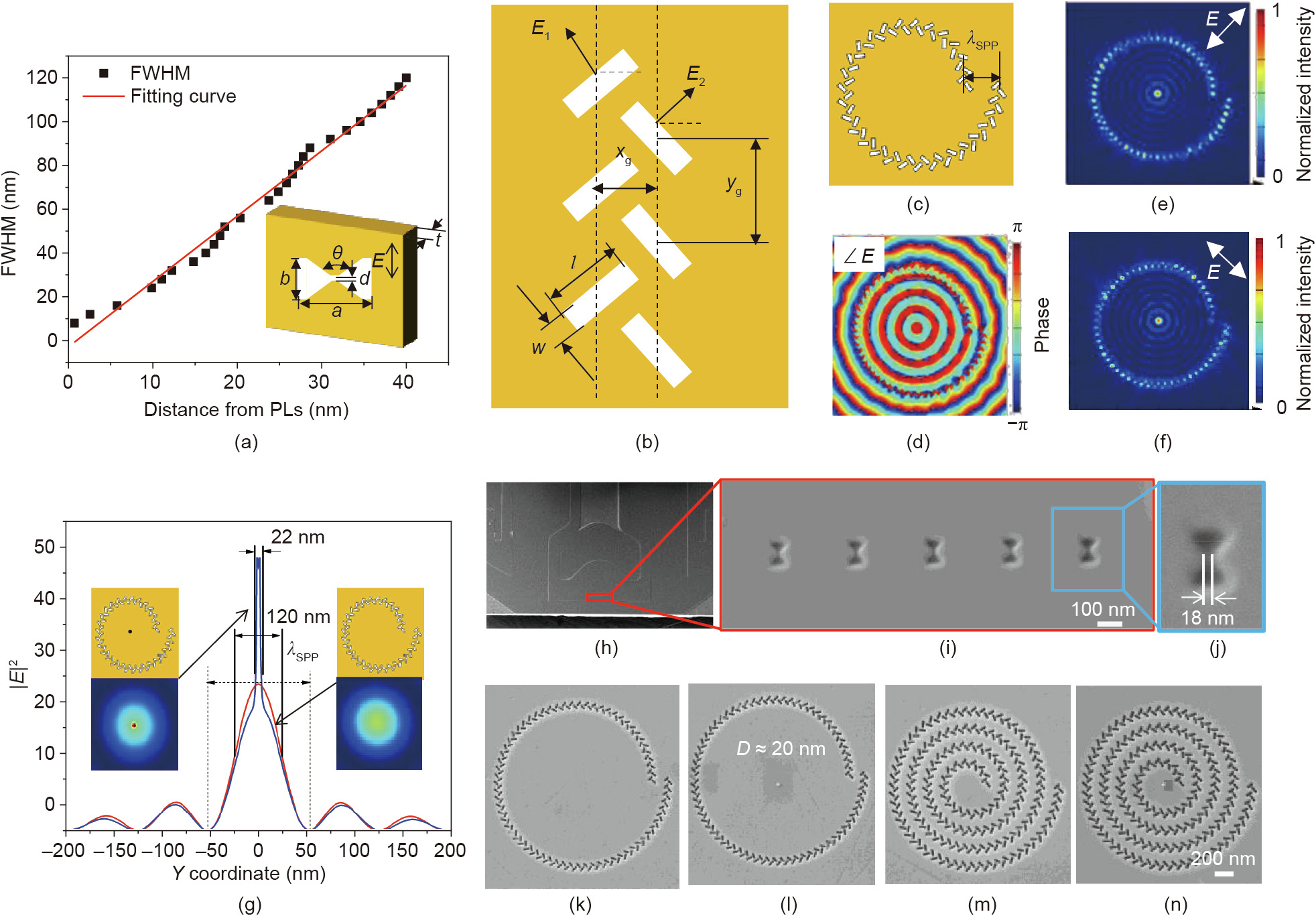
Fig. 3. Design and fabrication of the PLA. (a) The relationship of the FWHM of the bowtie-shaped aperture as the near-field distance when the structure gap size d is 10 nm. FWHM: full width half maximum; a: the length of the bowtie; b: the angle of the bowtie; θ: theangle of the bowtie; t: the thickness; E: incident electric field. (b) Double-slit column design using the concept of metasurface for SPP excitation under any polarizations. w: width of the slits; l: lengh of the slits; E1, E2: electric fields of the SPPs; xg: the distance of two columns of slits perpendicular to each other arranged parallel; yg: vertical spacing of the slits. (c) Double-slit array with the Archimedes spiral for central constructive interference. : wavelength of the SPP. (d) Phase distribution shows central constructive interference. (e, f) Normalized intensities under different linear polarizations show the same confined spot at the center. (g) Performance of multi-stage PL with a nano-cylinder at the center compared to the metasurface PL. (h) Rear edge of the slider and the location of the PL array. (i–n) SEM images of the bowtie-shaped and metasurface-based PL. D: the diameter of the cylinder.
《3.4. Parallel nanolithography》
3.4. Parallel nanolithography
Our PPNL system is mainly established based on the HDF tester. Fig. 4(a) shows the part of the system. A laser diode with a wavelength of 404 nm (L404P400M, 0–600 MHz modulation, Thorlabs, USA) was used as the light source. The optical system and the PFH are fixed on the nano-stage (PI-V511, PI, Germany) with 1 nm absolute accuracy and 230 mm stroke that enables radial position control for simultaneous movement of the laser and the PFH to directly write over the entire radius of the substrate. Fig. 4(b) shows the magnified view of the PFH and substrate. The assembled PFH loads on the rotating substrate from the ramp when the fabrication starts. The photoresist used in the system is TeOx which is an inorganic thermal photoresist widely used in optical storage applications. A 260 nm thick TeOx film with roughness of 0.648 nm was sputtered on the substrate (Fig. 4(c)). Studies show that this film has the highest sensitivity when x is between 1 and 1.2. Fig. 4(d) shows the XPS analysis of x value under different oxygen and argon ratios in the sputtering process, and a ratio of 2:100 was chosen in the following experiments. To have better tribological properties on the surface of the photoresist, a layer of PFPE lubricant is coated on the surface. To verify the effectiveness of the photoresist, the microscale direct laser processing without a PFH is first demonstrated in Fig. 4(e), where the lithography results after exposure and 30 s after development are shown. Before development, due to the high laser power, it will cause ablation of the photoresist surface shown from the color difference when the line array is processed at a lower speed. As the speed increases, the ablation weakens and gradually disappears at 12.5 mm·s–1 . After 30 s development, the ablated lines become wider which is due to corrosion of phase change regions. The line with a speed of 12.5 mm·s–1 is also visible, which indicates that the temperature has reached the phase change temperature even though there is no line that can be observed after exposure. The non-exposed areas and line-edge color differences are due to slight depth differences caused by faster corrosion rates within the heat-affected zone. As the development time continues to increase, the width and depth changes are not obvious (Appendix Section S5), indicating that the 30 s development time has completely corroded the material in the phase change regions. Therefore, in the subsequent nanofabrication experiments, the development time was set to 30 s. Subsequently, PFHs with different PLAs were used in the PPNL system to perform the parallel nanolithography. Fig. 4(f) shows the processing SEM characterization results with bowtie-shaped and metasurface-cylinder type PLs. It shows that multiple lines can be processed simultaneously with PLA which demonstrates the effectiveness of parallel plasmonic lithography with our prototyping PPNL system. Atomic force microscopy characterization results in Fig. 4(g) shows lines with 35 and 26 nm width can be achieved by bowtie-shaped and metasurface-cylinder type PL, respectively. The structure depth is approximately 2–3 nm due to the exponential decay of energy of SPP.
《Fig. 4》
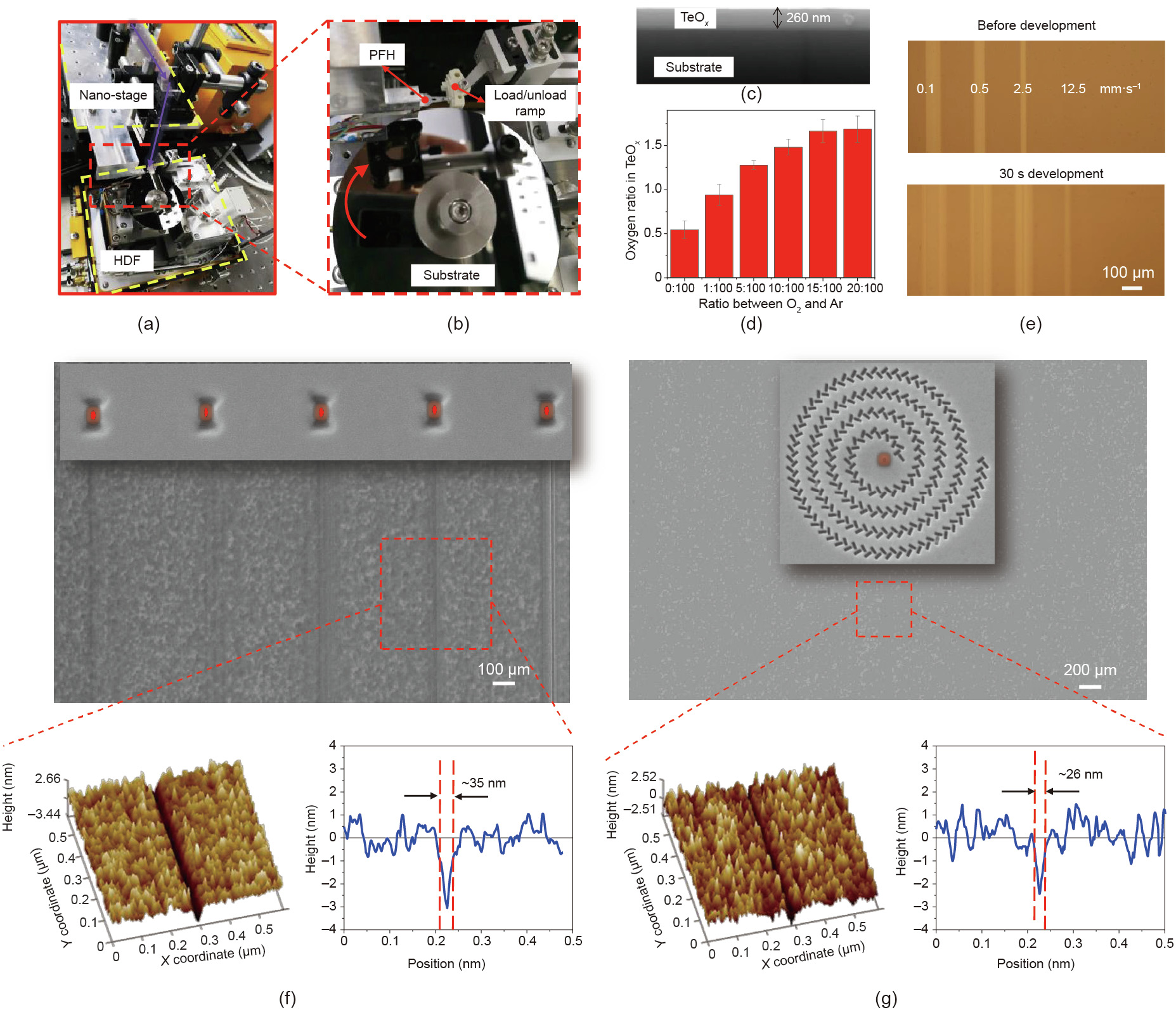
Fig. 4. PPNL system and parallel nanolithography. (a) Part of the PPNL system consisting of a nano-stage, optical system, and HDF tester. (b) PFH, the load/unload ramp, and the substrate. (c) Sectional view of the TeOx film on the substrate. (d) XPS analysis of x value under different oxygen and argon ratio. (e) The development experimental results of microscale direct laser processing without a PFH with different speed of nano-stage. (f, g) The SEM and atomic force microscopy (AFM) results of direct-writhing with bowtie-shaped PLA and metasurface-cylinder type PLA.
《4. Discussion》
4. Discussion
As demonstrated above, the aspect ratio of the plasmonic lithography structure is limited by the exponential decay nature of the evanescent components into the photoresist. A metal– insulator–metal scheme was demonstrated to improve the etching depth [35]. The same conclusion was also obtained by our simulation in Appendix A Section S6. For the silver–photoresist–silver structure, we found that a large aspect ratio and a small FWHM can be simultaneously achieved when the upper layer of silver is 10–20 nm and the lower layer of silver is around 40 nm. This scheme can achieve the deepest 50 nm photoresist etching. In addition, the system we built has the potential to realize the processing of arbitrary nano-patterns through suitable control strategies similar to the track seek control strategy [36] in the HDD (Appendix A Section S7). By obtaining circumferential positions with the rotation of the substrate and radial positions with the nano-precision translation stage, any positions in the substrate can be directly written by combining the laser switch with the electro–optic modulator. Furthermore, many of the cutting-edge technologies in the HDD industry can be introduced into the system. For example, according to the current state-of-the-art hard disk technology, heat assisted magnetic recording [37,38], the system can be further miniaturized to the size of the HDD by directly integrating the laser diode into the upper surface of the PFH. Thermal FH control [39] technology can reduce the local FH of the PL to the order of 1 nm to achieve smaller linewidth fabrication. Embedded contact sensor [40,41] can detect the FH for high flying feedback to ensure the fabrication uniformity. Recently, an evanescent Bessel beam with sub-diffraction characteristics is generated by using a hyperbolic metamaterial composed of alternate metal and dielectric layers to launch the bulk plasmon polaritons [42]. It showed that the evanescent Bessel beam with a central spot size of 62 nm could be maintained for a distance as large as 100 nm that greatly reduces the distance requirement in the near field and provides another possibility for near-field lithography.
《5. Conclusions》
5. Conclusions
In summary, we have demonstrated a high-speed PPNL prototyping system. With careful design, a novel PFH with good static, dynamic, and load/unload performance is obtained to achieve around 15 nm FH and around 63 μrad pitch angle over the whole substrate range at a speed 8–18 m·s–1 . In addition, a multi-stage metasurface-cylinder PL is proposed for polarization independent excitation of the PSP and LSP to achieve 2x nm FWHM. With such key components, the system is established and around 26 nm linewidth is achieved. The proposed parallel nanolithography system is a reliable nanofabrication system with high throughput (around 109 μm2 ·h–1 ), low cost, and high freedom, which has the potential for wide applications in fundamental research and nano-devices prototyping.
《Acknowledgments》
Acknowledgments
We acknowledge the financial support by the National Natural Science Foundation of China (91623105 and 52005175) and Natural Science Foundation of Hunan Province of China (2020JJ5059).
《Compliance with ethics guidelines》
Compliance with ethics guidelines
Yueqiang Hu, Ling Li, Rong Wang, Jian Song, Hongdong Wang, Huigao Duan, Jiaxin Ji, and Yonggang Meng declare that they have no conflict of interest or financial conflicts to disclose.
《Appendix A. Supplementary data》
Appendix A. Supplementary data
Supplementary data to this article can be found online at https://doi.org/10.1016/j.eng.2020.08.019.


 京公网安备 11010502051620号


