

《1. Introduction》
1. Introduction
Recent interest in the fifth generation (5G) network communication [1–3] operating in the Ka-band—that is, millimeter waves—stems from the fact that it is expected to provide a much higher data rate in the gigabit range, which is impossible to achieve using current wireless services [3]. The millimeter-wave (mmwave) phased-array antenna is certain to play an important role in 5G applications, thanks to its many desirable attributes, which include high gain [3,4], a higher transmission rate, and shorter latency. Recently, several studies of mm-wave phased-array designs for 5G applications have been reported in Refs. [5,6]. The phased-array configuration has been proposed to serve the user in densely populated areas by reducing interference and thereby realizing a high communication rate between the base station and mobile devices. In addition, it has been argued that beamswitching is essential to address the challenges of future 5G applications [7–9] at millimeter waves, since it offers high-power efficiency and large channel capacity with wide-angle scan coverage. The low-profile antenna array design, presented in Refs. [10–13], provides good performance at high frequencies; however, it can only scan the beam in one plane using mechanical means [10]. Recently, beam-switching networks using structures such as a substrate-integrated waveguide [12], Butler matrix [13], printedridge gap waveguide [14], and magneto-electric dipole antenna array fed by a ridge gap waveguide (RGW) Butler matrix [15] have been proposed by the research community. A one-dimensional (1D) beam-scanning technique is proposed in Ref. [9], which utilizes mechanical rotation and whose performance in terms of gain, sidelobe level (SLL), and so forth, varies with different orientation angles. More recently, a forthcoming publication [16] is expected to serve as a good reference source for fixed-beam and scanned arrays. In the present work, we discuss two different strategies for designing scanning arrays, both of which circumvent the use of conventional phase shifters to achieve beam scanning. This is an important feature that is highly desirable in the mm-wave range because conventional phase shifters are both lossy and costly. A quick-fix solution to this problem is to use an active phase shifter that includes a radio frequency (RF) amplifier. While this solution ameliorates the loss problem, it unfortunately exacerbates cost issues. Furthermore, it makes the antenna system powerhungry, which is obviously undesirable. Realizing high levels of gain in these scanning antennas and maintaining this gain while an antenna scans over a wide range of look angles is desirable, and we address this important design issue in this work. We begin with aperture antennas with slotted waveguide arrays that are widely used for high-frequency applications because they provide high gain, wide bandwidth, a low profile [17–21], and relatively simple configurations [22]. The literature (e.g., Refs. [17,23]) is replete with descriptions of low-profile aperture antennas that are potentially suitable for the present application. However, the need for improved designs of these antennas operating in the mm-wave regime remains [24] and, in this work, we present two types of design that appear to show promise over legacy designs such as conventional phased arrays [25], convex or flat lenses [26], Rotman lenses [27], metasurface-based reflectarrays [28], and arrays with a Butler matrix [29].
《2. Arrays with wide-angle scan capability》
2. Arrays with wide-angle scan capability
In this section, we present two designs of wide-angle scanning arrays, both exciting a Luneburg lens, using feed structures to realize a scan range of –φ to +φ in azimuth (where φ is azimuthal angle) and +θ to –θ in elevation (where θ is polar angle), and both wide, on the order of 40° (elevation) to 50° (azimuth). The first design utilizes a flat-base waveguide array feed with a pigeonhole configuration, which has been reported in Ref. [30]. The second design employs a patch array for the feed, together with switching circuits, in order to achieve signal coverage over a wide area by switching a narrow beam of the patch-fed lens in a rasterscan fashion. The basic working principle of the Luneburg lens antenna when it is operating in the receive mode is shown in Fig. 1. The lens has a radially varying relative permittivity (εr) profile, given below in Eq. (1), to focus an incident plane wave at a point diametrically opposite to that of the incident side when the lens operates in the receive mode. The profile is given by the following equation:

where r is the distance from the center of the lens, and R is the radius of the lens.
《Fig. 1》

Fig. 1. The principle of operation of a Luneburg lens. r: the distance from the center of the lens; R: the radius of the lens; O: focus.
An 11-layer Luneburg lens was presented in Ref. [30] through simulations, in which the lens was fed at its base by a 6 × 6 array of waveguides. The specified diameter (2 × R) of this lens was 63.5 mm. It had ten inner layers, each 3 mm thick, while the outermost layer was 1.75 mm thick. The permittivities of the different layers varied according to Eq. (1). The dielectric constant was 2.0 at the core and 1.05 at the outermost layer. Beam scanning was accomplished by switching the ‘‘on” and ‘‘off” feeds located at the bottom of the guides, one at a time, to point the beam in the desired direction. It was shown in Ref. [30] that this Luneburg lens design could scan up to 72° from the boresight in both the azimuth and elevation with little degradation of the pattern and with a relatively small scan loss. A similar design is shown in Fig. 2, where a 5 × 5 array of waveguides is used. A typical radiation pattern realized by exciting one waveguide is shown in Fig. 3.
《Fig. 2》

Fig. 2. The designed Luneburg lens: (a) isometric view; and (b) top view.
《Fig. 3》
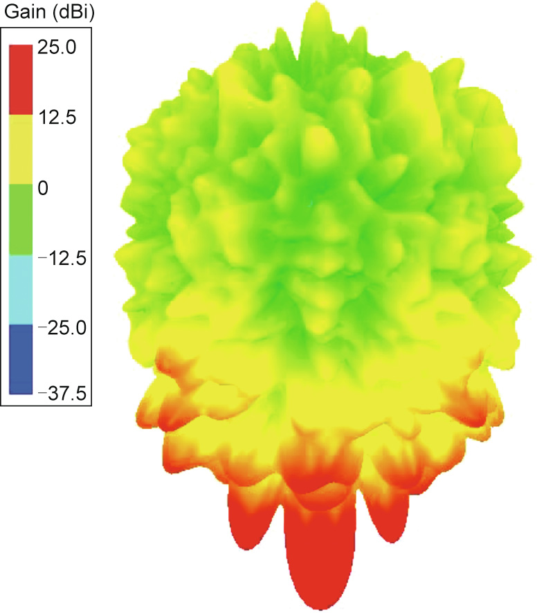
Fig. 3. Radiation pattern of the Luneburg lens antenna when one waveguide (waveguide 13) is excited. dBi: the gain relative to an isotropic antenna.
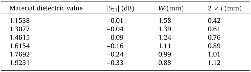
For ease of fabrication, it is desirable to reduce the number of layers of the Luneburg lens without compromising its performance. It is necessary to optimize the permittivity profile in order to achieve this reduction, rather than just sampling the continuous profile as was done in the original 11-layer case. The optimized profile [31,32] is presented in Table 1 (see Column 1).
It is not uncommon to find that the required materials, as listed in Table 1, are not commercially available off the shelf (COTS). To address this problem, an obvious approach is to employ artificially synthesized dielectrics to fabricate the lens. Two different techniques [33,34] that can be used for this purpose are described below. The first of these techniques employs the process of laser drilling (i.e., machine drilling), while the second relies on additive manufacturing (i.e., three-dimensional (3D) printing).
《Table 1》
Table 1 Unit cell size properties for different lens layers.
dB: decibel; |S21|: transmission coefficient; W: the width of air void;  : the width of dielectric column in unit cell.
Method 1: Laser-cutting holes in the dielectric for lens design. For laser cutting or machine drilling, we use readily available dielectric boards and drill holes in the dielectric sheet [34] to synthesize the permittivity values of the spherical shells specified in Table 1. Either laser or computer numerical control drilling may be used for this purpose, both of which are well-established techniques. The Luneburg lens fabricated by using the holey-sheet approach consists of many layers, with the number of layers determined by the thickness of the dielectric sheet material and the diameter of the lens. Considerable care must be exercised to determine the hole pattern, which changes from sheet to sheet as we go up the sphere from its equator to its pole. It is necessary to numerically simulate the holey discs to ensure that the perforated discs accurately mimic the artificial dielectric rings that we are attempting to synthesize, since the simplistic estimates of the effective dielectric constant of the stacked holey discs, which are based on classical effective medium theories, are insufficiently accurate.
Method 2: 3D printing of the lens. An alternative scheme for synthesizing artificial dielectrics is to use 3D printing. The theoretical basis for designing artificial dielectrics may be found in Refs. [35,36] and is omitted here.
Thermoplastic polylactic acid (PLA), which has a permittivity (εr) of 2.72, is a very common material used for 3D printing and is used in the present design. In this approach, we modify the permittivities of a COTS material by inserting air voids in it to realize the required permittivity, as listed in Table 1. To illustrate the lens design, we choose a unit cell with a periodicity of 2 mm × 2 mm and use unit cells consisting of air voids and dielectrics, as shown in Fig. 4. The designed unit cells, together with their required dimensions, are also presented in Table 1. The designed cells have better than 0.4 decibel (dB) insertion loss.
Apart from the methods discussed above, another way to design the Luneburg lens is to use dielectric materials with varying permittivities. Such a lens was fabricated using the desired permittivities called for in the Luneburg lens design by using different dielectric materials, as shown in Table 1, Column 1. The diameter of the six-layer lens is 14.5 cm and the antenna operates from 24 to 28 GHz. The simulated |S11| (|S11| is reflection coefficient magnitude) and the realized gain of the lens are shown in Figs. 5(a) and (b), respectively. It is important to note that this type of design can be expensive to fabricate, since the desired permittivities must be specifically realized by mixing different dielectric materials. The weight of this lens was found to be 1.2 kg after fabrication.
《Fig. 4》

Fig. 4. The unit cell of the Luneburg lens (different views): (a) top view; and (b) perspective view.
《Fig. 5》
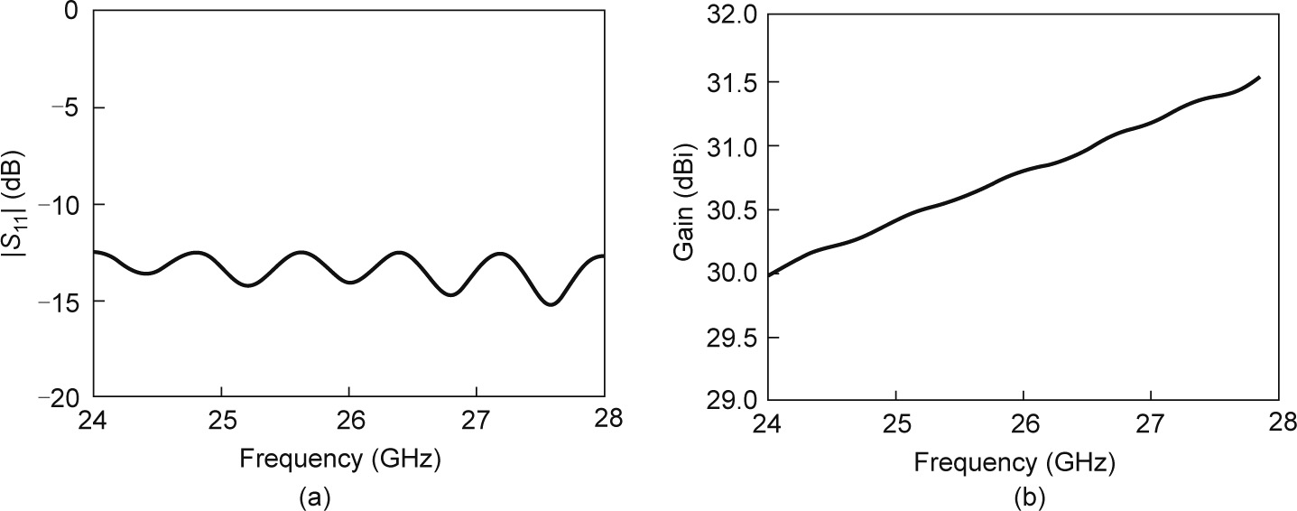
Fig. 5. Simulated response of the Luneburg lens: (a) |S11|; and (b) realized gain.
Fig. 6(a) shows the measurement setup for the Luneburg lens with an open-ended waveguide feed. Figs. 6(b) and (c) show the normalized radiation patterns for the lens at 26 GHz for a φ = 0° cut and a φ = 90° cut, respectively. The simulated gain of the lens at 26 GHz is 30.7 dBi (where dBi represents the gain relative to an isotropic antenna), while the measured gain was found to be 29.2 dBi. We also found that the lens provides a consistent gain of 29.2 dBi along the broadside, and the gain is maintained at this level even for wide scan angles; that is, the scan loss is minimal, which is an important advantage of the Luneburg lens.
《Fig. 6》
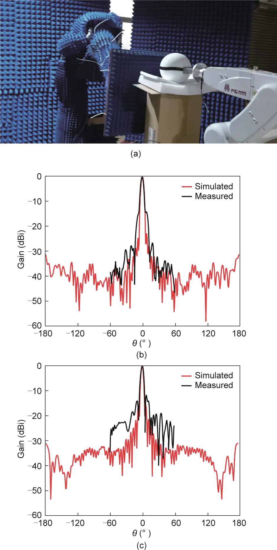
Fig. 6. Measurement setup and radiation patterns of the 14.5 cm, 6-layer Luneburg lens antenna: (a) measurement setup; (b) φ = 0° cut; and (c) φ = 90° cut.
To reduce the cost and ease the fabrication, the PLA infill method was used to design the lens with a diameter of 14.5 cm. The outer sixth layer of the lens was not 3D printed; instead, foam with a permittivity of 1.15 was used. However, the inner five layers were 3D printed. The 3D-printed lens (inner five layers) is shown in Fig. 7.
《Fig. 7》
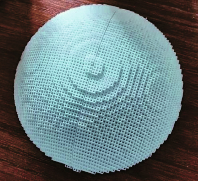
Fig. 7. 3D-printed Luneburg lens.
A 5 × 5 conformal patch array (Figs. 8 and 9) was designed to feed the Luneburg lens, as shown in Fig. 10, in order to verify its scan performance. The edge-to-edge separation distance between the adjacent elements of the array was chosen to be 1 mm. The conformal array (Fig. 9) was placed on the surface of the Luneburg lens for excitation, as shown in Fig. 10. The reflection and isolation coefficients were found to be better than 10 dB throughout the frequency band of 24–28 GHz. Beam scanning was accomplished by switching the feed elements (i.e., patches) for the lens, one at a time, in order to point the beam in the desired direction. The two-dimensional (2D) simulated radiation pattern for the φ = 90° cut is shown in Fig. 11. Similar behavior was observed for the 2D simulated radiation pattern for the φ = 0° cut, which is shown in Fig. 12. Figs. 11 and 12 show the beam scanning performance when particular port out of ports (Port 0–Port 8) are used. It is important to note that the maximum scan angle is ±12°, because the array size is relatively small. A larger scan range could be realized by increasing the size of the feed array.
《Fig. 8》
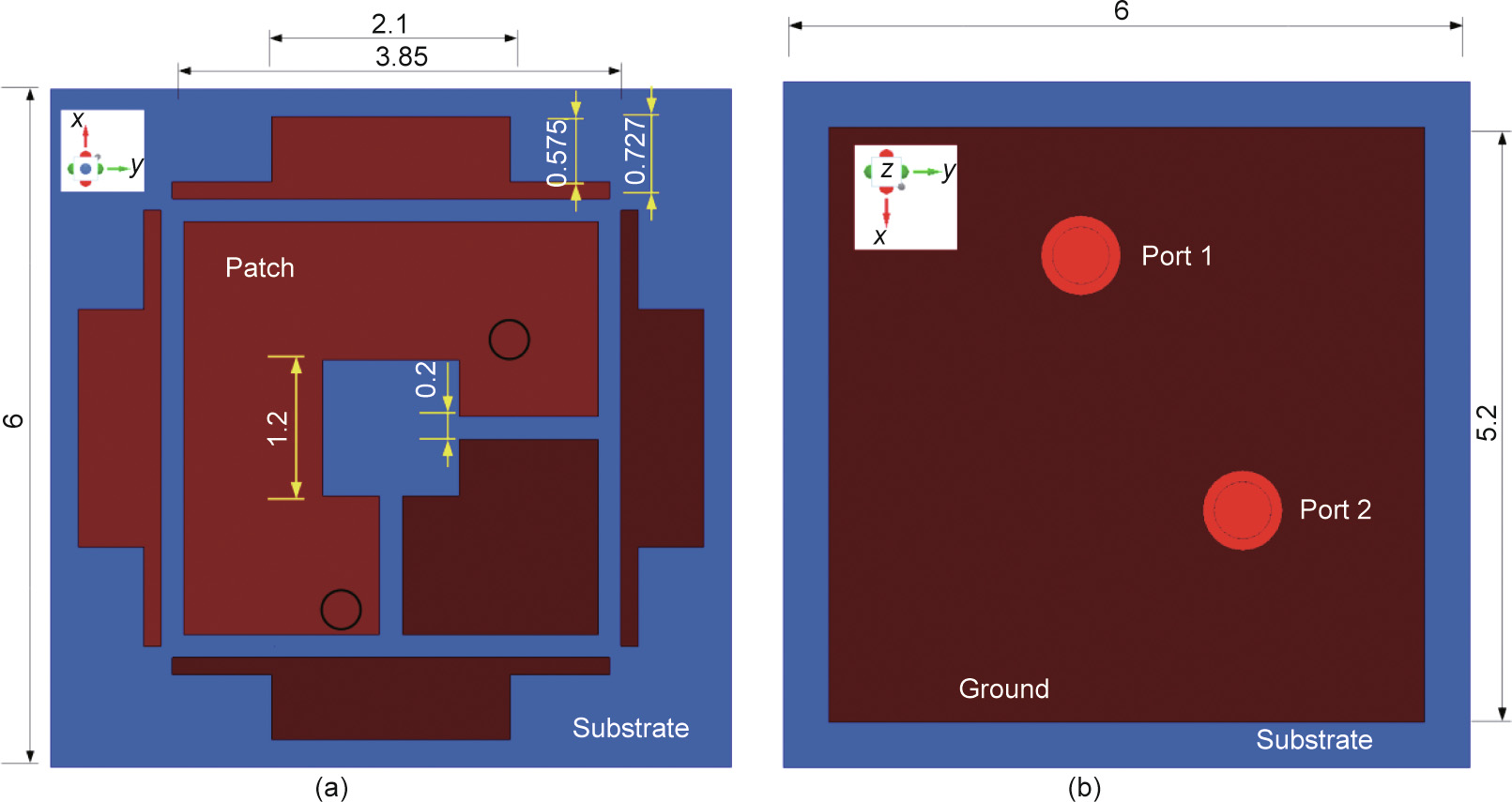
Fig. 8. Single-patch antenna element with a dual-polarization feed (all dimensions are in millimeters): (a) top view; and (b) bottom view.
《Fig. 9》

Fig. 9. A 5 × 5 conformal array: (a) bottom view; and (b) top view.
《Fig. 10》

Fig. 10. A 5 × 5 conformal array exciting a Luneburg lens: (a) top view; and (b) front view.
《Fig. 11》
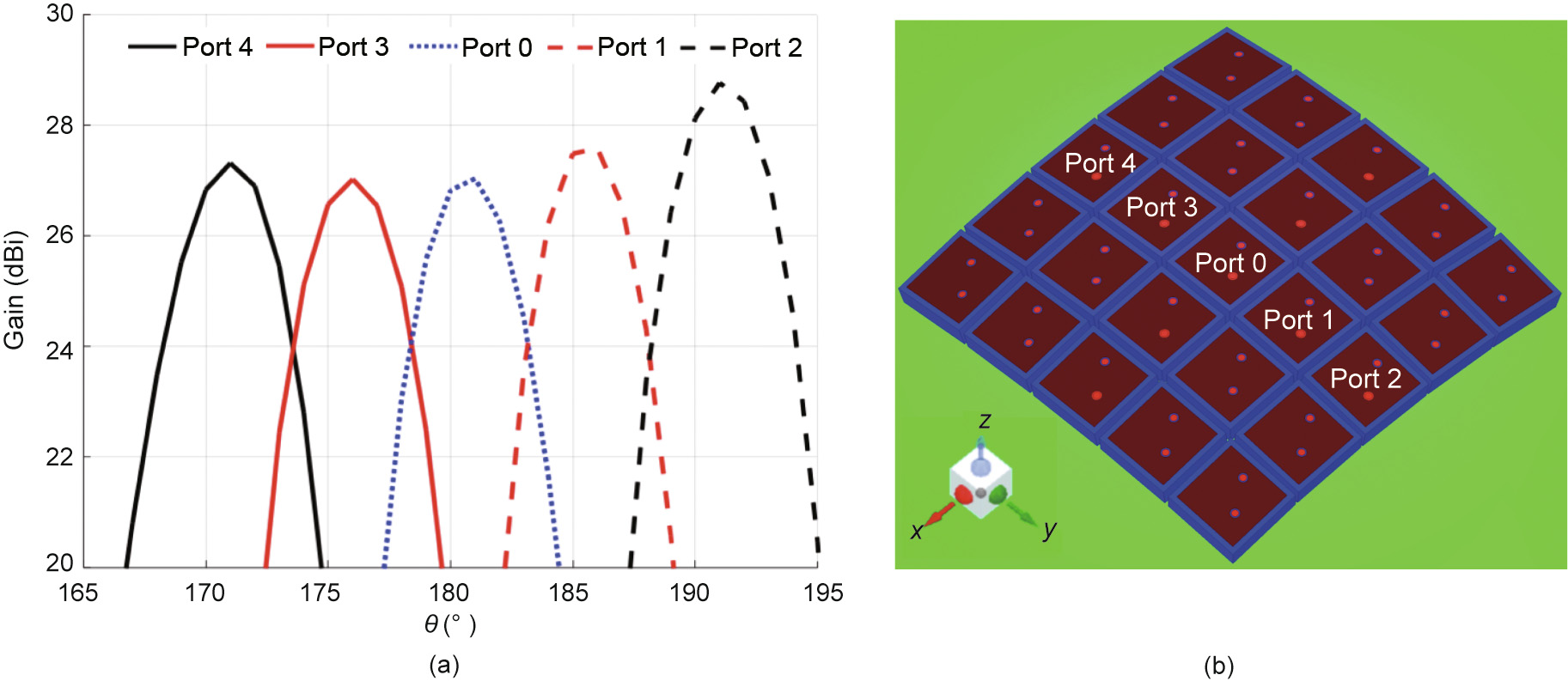
Fig. 11. 2D simulated radiation pattern at φ = 90°. (a) Gain response for different active feed elements; (b) location of different active feed elements.
《Fig. 12》

Fig. 12. 2D simulated radiation pattern at φ = 0°. (a) Gain response for different active feed elements; (b) location of different active feed elements.
While the 3D-printed method is very versatile, it is challenging to maintain the accuracy of the building blocks of the lens, shown in Fig. 6 above, due to the need to control the fabrication tolerances to within fractions of a millimeter. This prompted us to revisit Method 1, described above, and fabricate the lens by stacking sheets of pure blue material with εr of 2.47, in which holes were drilled to artificially synthesize the desired dielectric materials for the lens, which were presented earlier in Table 1. Fig. 13(a) shows the spherical lens without the outermost layer, for which we used a ‘‘real” material—more specifically, a foam-type material with a permittivity close to 1.15. Figs. 13(b) and (c) show two different discs together with their hole patterns, the first of which is at the equator, while the second is closer to the pole. Altogether, 90 of these ‘‘holey” discs are required to form the sphere, without the outermost shell.
The 2D scanning beam of an aperture array at the desired operating frequency is not the last design challenge of aperture arrays for 5G, for which polarization diversity may also be required. Most of the antenna array based on waveguides has a linear polarization along the desired frequency range. As the circular polarization of an antenna array is so important for the network communication applications, the steps to achieve a circular polarization from the linear and dual-linear polarization of electromagnetic waves are presented in the next section.
《Fig. 13》
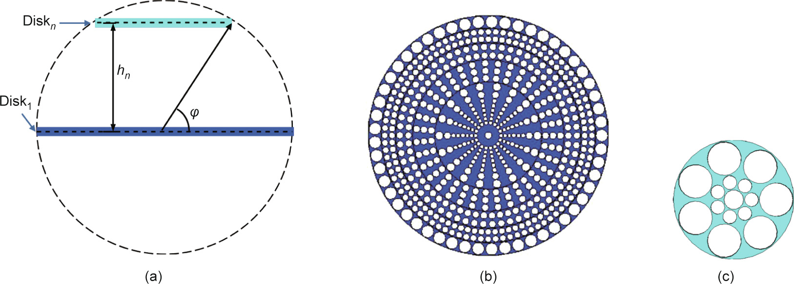
Fig. 13. Alternate lens design. (a) Location of the different discs. hn; height of nth disk; n: number of disk; Diskn: nth disk. (b) Disc cut near the center of the lens. (c) Disc at the extreme end of the lens.
《3. Beam scanning of a slot array in a substrate integrated waveguide (SIW)》
3. Beam scanning of a slot array in a substrate integrated waveguide (SIW)
《3.1. Beam scanning of an SIW array using electronically switched phase shifters》
3.1. Beam scanning of an SIW array using electronically switched phase shifters
For 5G communications systems, a plethora of beamforming techniques have been proposed in recent years to meet the challenges encountered when attempting to replace conventional phase shifters, which are both costly and power-hungry when combined with active circuits to mitigate the loss problem. In this work, we propose a novel technique for realizing the desired phase shift by modifying the electrical path length between two consecutive radiating elements using electronic switching circuits. The phase shifter is realized in an SIW by introducing curved sections of the guide between the radiating elements and modifying the effective lengths of these sections by switching the vias ‘‘on” or ‘‘off” using PIN diodes or varactor diodes. We propose two different methods to realize the desired phase shifts. The first method entails a change in the wave path through the curved sections by altering the positions and number of vias in these sections (Figs. 14 and 15); the second accomplishes a change in the path length through the curved section by activating or deactivating the PIN diodes placed in these sections. Fig. 16 demonstrates the equivalent circuit of the PIN diodes (MA4AGFCP910, MACOM, USA) controlling the switching mechanism. Fig. 14 presents the dimensions of the radiating element. The separation distance between two consecutive slots (b in Fig. 14) is equal to 6 mm (close to half wavelengths), while the slot length and width (c and e) are equal to 2.88 and 0.5 mm, respectively. The shape of the slot differs from the conventional rectangular or circular geometries and is optimized to maintain the reflection coefficient (S11) below the level of –10 dB in the operating frequency range.
《Fig. 14》

Fig. 14. Radiating element shape. b = 6 mm; c = 2.88 mm; e = 0.5 mm. b: the separation distance between two consecutive slots; c: the slot length; e: the slot width.
《Fig. 15》

Fig. 15. The proposed slotted SIW curved array. (a) An example of the phase shifter; (b) one SIW curved section containing all the switches in colors that are turned ‘‘on” or ‘‘off” depending on the required phase shift.
《Fig. 16》

Fig. 16. The proposed slotted SIW curved array. (a) An SIW curved section containing all the switches; and (b) a PIN diode. R: resistance, L: inductance; C: capacitance.
Fig. 17 presents the reflection coefficients at the input port of the excitation for different phase-shifter configurations, which are designed to ensure that the S11 of the array is always less than –10 dB in the desired frequency range, regardless of the phase-shift level. Fig. 18 illustrates the scan capability of the curved SIW (CSIW) phase shifters. The figure shows that the simulated gains of the seven different phase shifters vary between 9.5 and 11.1 dB, and a beam scanning of up to 104° can be achieved in the longitudinal plane.
《Fig. 17》

Fig. 17. Reflection coefficient of all phase shifters.
《Fig. 18》
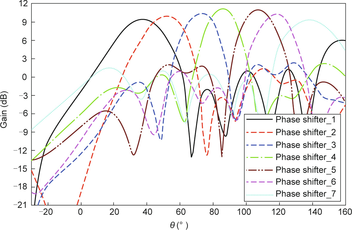
Fig. 18. Scan performance of phase shifters inserted in the curved SIW.
《3.2. Gain enhancement using metallic wings》
3.2. Gain enhancement using metallic wings
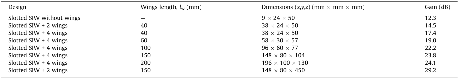
Next, we investigate ways to enhance the gain of the proposed CSIW scanning array described in the previous section. To this end, we turn to Fig. 19, which shows two metallic wings added to the two sides of the abovementioned array configuration. Our goal is to increase the effective aperture of the array in the transverse plane, thereby narrowing the beam in this plane and increasing the gain of the array. Fig. 20 shows the array geometry, in which two additional wings have been added to the two ends of the array—front and back—to further improve the performance. The relevant dimensions for the winged-array design are provided in Table 2, together with the results for the gain enhancements achieved by the array.
《Fig. 19》
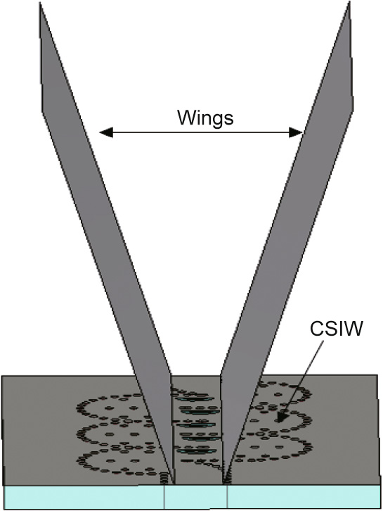
Fig. 19. CSIW with two metallic wings.
《Fig. 20》
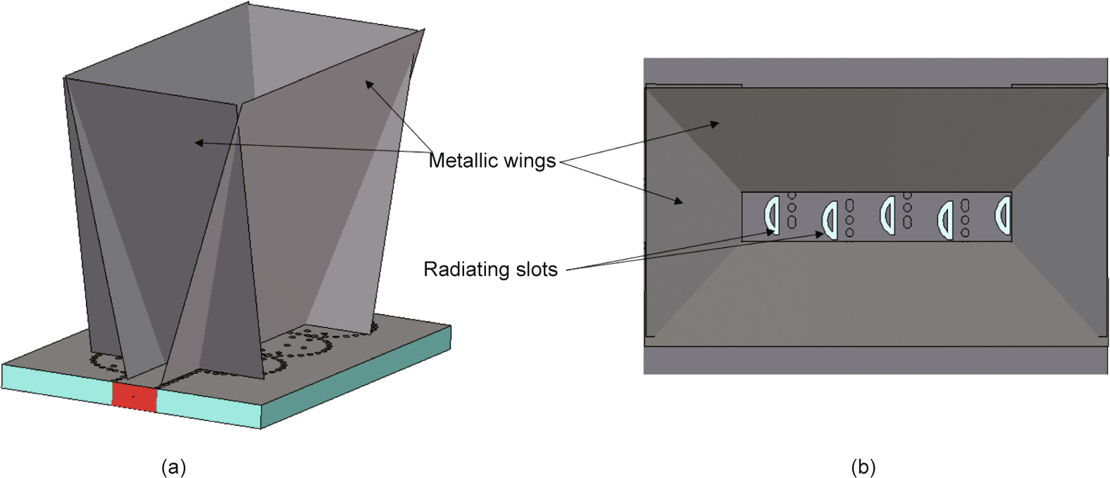
Fig. 20. CSIW with four metallic wings: (a) perspective view; and (b) top view.
《Table 2》
Table 2 Variation in gain at 26 GHz.
《4. Wide-angle beam scanning using a tilted panel》
4. Wide-angle beam scanning using a tilted panel
《4.1. Beam scanning in the transverse plane》
4.1. Beam scanning in the transverse plane
In Section 2, we presented some SIW-based array designs with switchable phase shifters, which control the tilt angle of the main beam of the array in the longitudinal plane. In this section, we examine ways to scan the beam in the transverse plane. We then propose a new scheme for accomplishing this goal. In the scheme displayed in Fig. 21, we can scan the beam by varying the angle of the panel. Moreover, we vary the direction of the main lobe by tilting the panel instead. Fig. 22 presents the scan performance of the proposed scheme at an operating frequency of 26 GHz. We observe that a scan range of more than 120° can be achieved with little or no pattern degradation or scan loss. While the principle of beam scanning, upon which the proposed scheme is based, is relatively straightforward, the challenge is to design a panel such that its tilt angle can be changed electronically, rather than mechanically, to achieve the speed with which we want to scan the beam, which should be on the order of milliseconds or even microseconds, as opposed to seconds. Currently, work is in progress to investigate several different options, including reconfigurable metasurfaces and reconfigurable reflectarrays. Using liquid metals for the same purpose is an attractive alternative for applications in which relatively slow switching speeds are acceptable.
《Fig. 21》
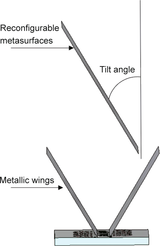
Fig. 21. 2D beam scanning using a tilted panel.
《Fig. 22》
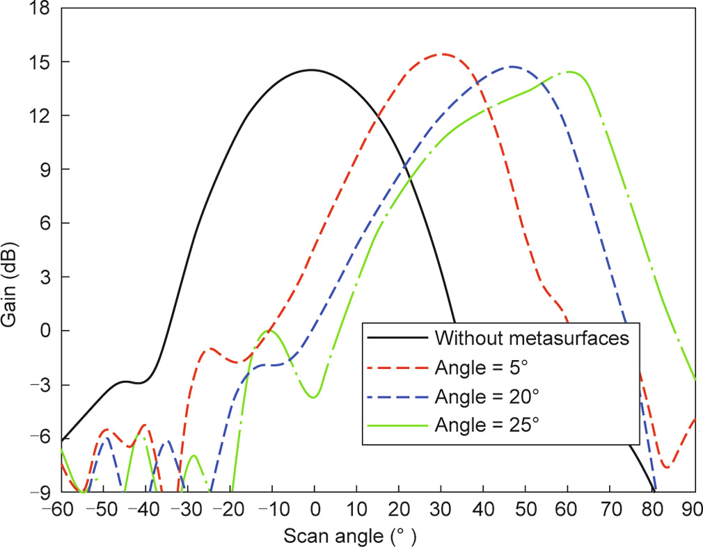
Fig. 22. Scan performance in the transverse plane using panel tilt.
《4.2. Beam scanning in the longitudinal plane》
4.2. Beam scanning in the longitudinal plane
For longitudinal scanning, we have previously discussed curved SIWs with phase shifters, consisting of electronically switched vias. To scan in the transverse plane, we can use reconfigurable tilted panels located above the array, as illustrated in Fig. 21. We can also use a similar panel—or even the same one—to scan in the longitudinal plane, as shown in Fig. 23, albeit with less flexibility than that provided by the phase shifters inserted in the SIW guide.
《Fig. 23》
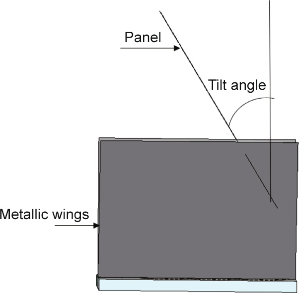
Fig. 23. Side view of the curved SIW array antenna with two metallic wings and a tilt panel.
《5. Gain enhancement of a slotted waveguide array using a grooved mounting platform》
5. Gain enhancement of a slotted waveguide array using a grooved mounting platform
《5.1. A modified slotted waveguide antenna array (SWAA) with grooved metallic wing structures》
5.1. A modified slotted waveguide antenna array (SWAA) with grooved metallic wing structures
In this section, we present a novel technique for enhancing the gain of an SWAA by modifying the platform on which the array is mounted. The technique is based on a recent publication [36], in which the authors first design a conventional slotted waveguide, and then add groove structures on both sides of the array to enlarge the effective radiating aperture of the array and thereby enhance the gain.
Next, we explore the possibility of further enhancing the gain up to the 30 dB level, which is desirable in certain applications of this type of antenna array, such as a base-station antenna element. We begin by increasing the number of slots from 27 (as in Ref. [36]) to 41, as shown in Fig. 24, and stretching the length of the array by 124 mm to accommodate this increase in the number of slots. Although this modification improves the gain up to the level of 29 dB (Fig. 25), it does not quite reach our goal of a 30 dB gain.
《Fig. 24》
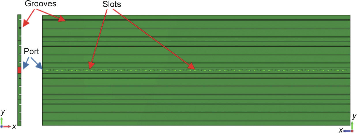
Fig. 24. An SWAA prototype with metal grooved structures.
《Fig. 25》
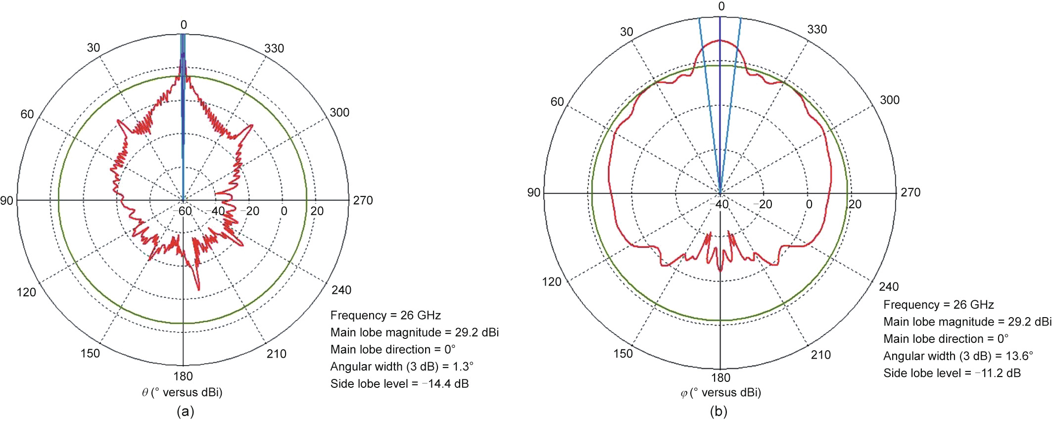
Fig. 25. Radiation patterns of an extended SWAA with grooves at 26 GHz: (a) H-plane; and (b) E-plane.
To further enhance the gain, our next step is to modify the geometry of the array in Fig. 24 by folding the extensions of the two sides of the original array, as shown in Fig. 26. This modification not only reduces the footprint of the antenna by a factor of two, but also helps to boost the gain to the desired goal of 30 dB, as shown in the plots for the radiation pattern presented in Fig. 27.
《Fig. 26》
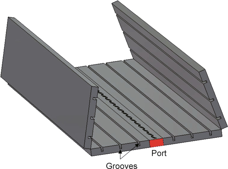
Fig. 26. Modified SWAA with metal grooved structures and wings.
《Fig. 27》
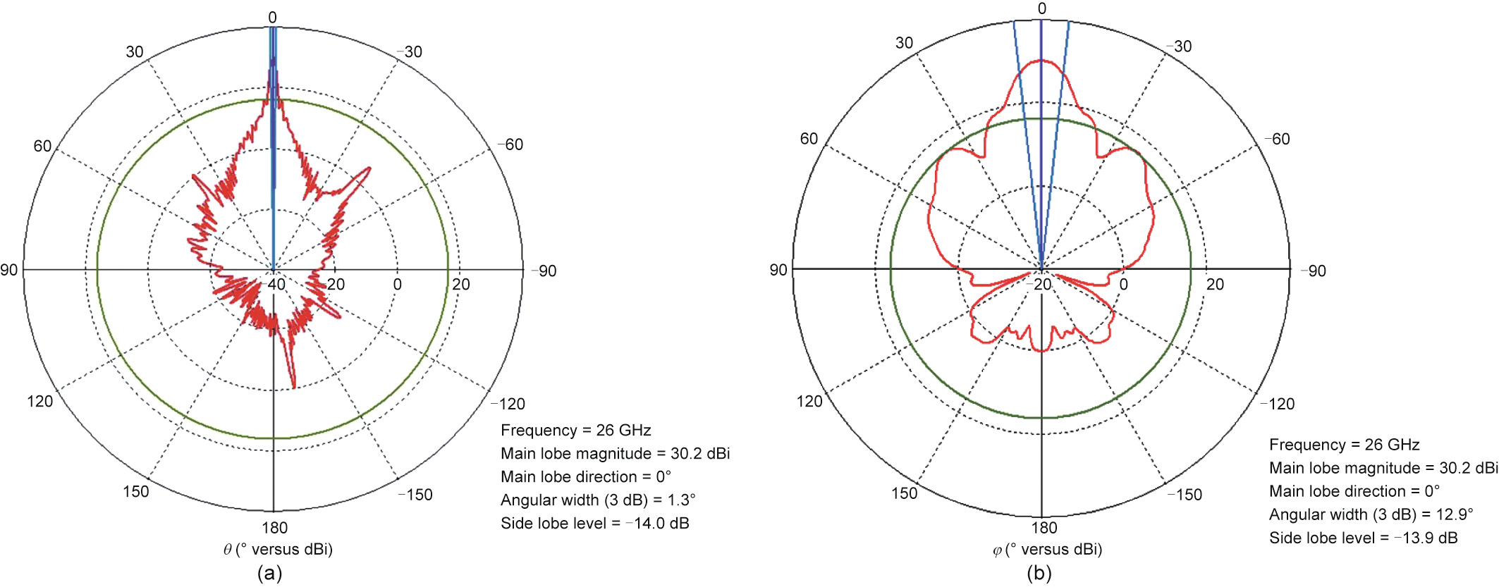
Fig. 27. Radiation patterns of a modified grooved SWAA with wings at 26 GHz: (a) H-plane; and (b) E-plane. Here, the E-plane and H-plane are reference planes for linearly polarized antennas.
The dimensions and the performance characteristics—namely, the gain and SLLs—of the original SWAA and two modified versions are summarized in Table 3 [36].
《Table 3》
Table 3 Variation in gain at 26 GHz.

《5.2. Beam scanning of an SWAA with grooves by using a tilted panel》
5.2. Beam scanning of an SWAA with grooves by using a tilted panel
Finally, we turn to the problem of scanning the array whose design was described in the previous section. In comparison with the case of the curved SIW array described in Section 3, we once again opt for the tilted panel approach to scan, as described in Section 4, rather than using phase shifters that are complex, lossy, and difficult to insert between the radiating elements. As mentioned earlier, we can fabricate these panels by using either reconfigurable metasurfaces or liquid metals, depending on the desired scan speed. The proposed geometry for the scanning array is shown in Fig. 28, and the radiation pattern for one tilt angle of the panel is displayed in Fig. 29. The radiation patterns show that a wide scan range can be achieved with little or no pattern degradation or scan loss. Furthermore, the variation of the panel angle has no significant effect on the impedance match. The tilt angle can be varied either mechanically or by using a reconfigurable panel comprising a metasurface loaded with varactor diodes, for example.
《Fig. 28》
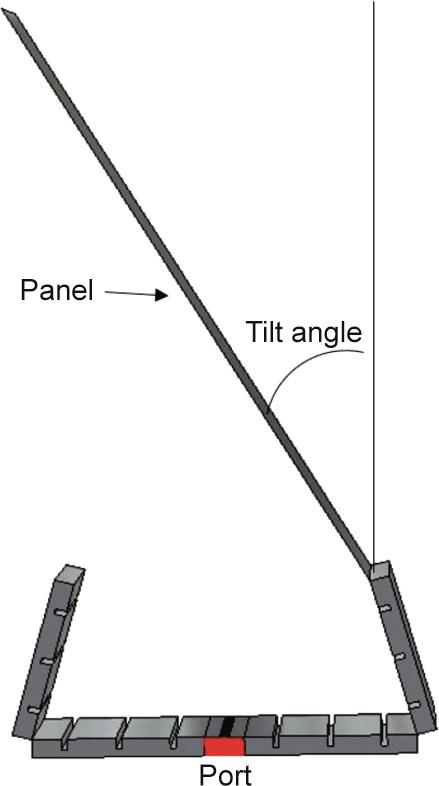
Fig. 28. A modified grooved SWAA with wings and a tilt panel for scanning.
《Fig. 29》

Fig. 29. Radiation patterns of a modified grooved SWAA with a tilted panel at 26 GHz: (a) H-plane; and (b) E-plane.
《6. Conclusions》
6. Conclusions
In this work, we reviewed several different designs of array antennas for both fixed-beam and scan applications. We presented a brief discussion of some legacy designs of arrays that achieve relatively low profiles in comparison with other high-gain antennas such as reflectors, reflectarrays, and conventional or flat Gradient-index lenses. Next, we described some novel design concepts that offer beam-scanning capabilities without the use of conventional phase shifters that are both lossy and expensive at millimeter waves. Our approach was either to replace the conventional ferrite-type phase shifters with switchable vias interposed between the array elements or to employ reconfigurable metasurface panels for scanning, with little or no scan loss. We also presented a Luneburg lens design, with an array feed comprising microstrip patch antennas for 2D scanning, which typically outperforms existing phased-array designs insofar as their scan performance is concerned, although it requires an array type of feed with switchable elements to scan the beam.
As a concluding remark, we mention that the design of highgain, low-profile, polarization-diverse, fixed-beam, and scanning antennas for 5G applications is a very active area of research and development. We hope that this paper will engender further interest in this area from researchers aiming to meet the challenges we have identified.
《Compliance with ethics guidelines》
Compliance with ethics guidelines
Raj Mittra, Abdelkhalek Nasri, and Ravi Kumar Arya declare that they have no conflict of interest or financial conflicts to disclose.


 京公网安备 11010502051620号


