

《1. Introduction: The role of adhesion in exploiting 1D materials》
1. Introduction: The role of adhesion in exploiting 1D materials
Owing in part to their uniquely high aspect ratio, large surfaceto-volume ratio, and low defect density, the remarkable mechanical [1,2], electrical [3–5], optical [6–8], piezoelectric [9], and magnetic properties [10] of one-dimensional (1D) materials have been of intense scientific interest for the past two decades. A diverse variety of 1D materials have been synthesized and characterized, including carbon nanotubes (CNTs) [11–13], boron nitride nanotubes (BNNTs) [14], bundled nanotube (NT) fibers and single-crystal nanowires (NWs) [15–23], coated/core–shell composite NWs [21], and polymer nanofibrils [22,24]. This now-mature research field has already shifted focus toward how to practically exploit the exceptional properties of 1D materials through their integration into batteries, fuel cells, and in solar-cell technology [25]; and their application as reversible dry adhesives and as strengtheners in structural composites. This introduction will clarify how the fabrication, functionality, and operational reliability of many of these technologies is in fact highly dependent on a not-so-well-studied property of 1D materials: their interfacial adhesion behavior.
1D materials have been integrated as functional components into a vast number of novel devices that have been both designed and demonstrated. These devices include field-effect transistors [21,22,24], transparent electrodes [20], energy harvesters [16], mechanical resonators [23], contact switches [26], force sensors [17], and biosensors and chemical sensors [18,19]. The application of 1D materials in probes for sensing and surface characterization was briefly reviewed by Mead et al. [27] in 2022. These devices, with their enhanced functionality, hold promise to disrupt entire industrial sectors, including disease diagnostics, wearable sensors, and implantable sensors in medicine; renewable energy generation and storage; and environmental monitoring for occupational safety. Yet, their commercialization has been hindered by the challenges associated with integrating 1D components into conventional microelectronics [28]. Integration not only affects device fabrication but also dictates functionality and reliability.
Device fabrication commonly necessitates the transfer, positioning, orientating, and fastening of 1D components at precise locations within microelectronic circuitry, in processes that are dependent on interfacial adhesion. Different device designs and operating principles require their 1D components to be integrated with a specific configuration, which in turn dictates what integration approaches can be implemented. Three configurations within previously demonstrated devices are provided as examples in Fig. 1 [18,21,23]. In the first configuration, a vertically aligned freestanding array or ‘‘forest” of Si NWs in a chemical gas sensor are clamped to a Si substrate at one end and to suspended graphene at the other, as shown in the diagram and scanning electron microscope (SEM) micrograph in Figs. 1(a) and (e), respectively [18]. In the second, partially suspended laterally oriented Rh NWs in a nanoresonator design are clamped at one end to a Au thin film, as shown in the diagram and SEM micrographs in Figs. 1(b), (d), and (f), respectively [23]. In the third, fully adhered parylenecoated InAs NWs in a field-effect transistor are fully adhered across Ni/Au contacts and a HfO2/SiO2 thin film, as shown in the diagram and SEM micrograph in Figs. 1(c) and (g), respectively [21].
《Fig. 1》

Fig. 1. 1D materials can be configured in different ways within a device. (a, e) Vertically aligned free-standing Si NW array within a chemical gas sensor: (a) schematic of heterostructure consisting of a Si substrate and suspended graphene; (e) scanning electron microscope (SEM) image of the NW–graphene interface through the electrontransparent graphene layer. (b, d, f) Laterally oriented Rh NWs partially suspended above Ti/Au contacts in a nanoresonator device: (b) schematic; (d, f) SEM images of (d) a single NW resonator with recognizable separation from the adjacent contact and (f) an array of resonators. (c, g) Laterally oriented (parylene-coated) InAs NW fully fastened across Ni/Au contacts and a HfO2/SiO2 substrate inside an NW field-effect transistor: (c) schematic; (g) SEM micrograph of the NW field-effect transistor. (a, e) Reproduced from Ref. [18] with permission; (b, d, f) reproduced from Ref. [23] with permission; (c, g) reproduced from Ref. [21] with permission.
Methods for NW integration via a ‘‘grow-in-place” strategy include template-assisted vapor–liquid–solid growth and solution growth [28,29]. Poor adhesion at the base of a 1D material may cause it to detach from the substrate, or strong adhesion between neighboring 1D materials in an array can cause them to clump together [30]. To achieve a laterally oriented configuration, a secondary ‘‘planarization” step, such as the ‘‘knocking-down” method, is required [31]. Methods for NW integration via a ‘‘grow-andplace” strategy include serial assembly via nanomanipulation (NM) and parallel assembly via dispersion and alignment in solution. NM-based transfer utilizes adhesive forces by regulating the interfacial area formed between the manipulator tip, donor substrate, acceptor substrate, and 1D material [32]. Effective parallel assembly in solution is dependent on the balance between the 1D material–substrate interfacial adhesion and the aligning force. Commonly employed aligning forces include shear force, dielectrophoretic force, magnetic force, and capillary action. Integration can also be achieved using nanocombing [33]; through dry, lubricated contact printing [32,34]; or via capillary-aided contact printing. Contact printing requires the adhesion of the acceptor substrate to be higher than that of the printing surface or donator substrate.
The operating principles of many devices are primarily dependent on the 1D component intermittently forming an interface, maintaining a dynamic interface, or avoiding interfacial formation. In vertically aligned triboelectric generators, the adhesion and friction behavior of the sliding contact between a ZnO NW tip and a zigzag-textured substrate dictate how the NW bends and ultimately influence electricity generation [16]. Defining the behavior of the adhesive contact formed between the end of a CNT-tipped microcantilever probe and a substrate is the key to interpreting topography micrographs produced during surface scanning in atomic force microscopy (AFM) [35,36]. Moreover, understanding the electrostatic interaction that occurs between the NW and the electrode surface in an NW-based contact switch is critical to predicting its switching behavior [26,37–39]. In addition, the interfacial adhesive strength of the 1D component within a device must be preserved through successive mechanical or thermal loadings over the device’s operational lifetime [40]. Moisture incursion from atmospheric humidity may also lead to interfacial delamination [41,42]. Reliability is of particular concern for flexible and electromechanical devices that experience high strain [43].
The interfacial adhesive behavior of 1D materials is also fundamental to the development of biomimetic adhesives. 1D arrays are being integrated into hierarchical structures that seek to mimic the incredible dry and reversible adhesive behavior of hierarchical structures found in nature [44]. More specifically, the compliant structure of gecko setae, as shown in Figs. 2(a)–(c) [45], is able to precisely conform to the topography of a surface, forming large interfacial contact areas and hence exhibit exceptionally high adhesion. Numerous biomimetic adhesive designs based on CNT arrays have been developed [46–58], and Hu et al. [44] provided a review on this topic in 2013. Figs. 2(d)–(g) [59,60] show hierarchical structures based on 1D arrays. The small cross-section and large surface areas of 1D materials are essential to the capability of a hierarchical structure to buckle, conform, and adhere to various surface topographies. However, the adhesive interactions that occur between NW arrays and textured surfaces are complex. Typically, the tips of numerous 1D structures in an array will adhere to a surface, each at a different contact angle, with different contact areas and differing contact forces.
《Fig. 2》

Fig. 2. (a–c) Hierarchical structure of a gecko toe. ST: seta; BR: branch; SP: spatula. (d, e) SEM micrographs showing a multiscale hierarchical structure containing CNT forests deposited on polymer micropillars. (f, g) SEM micrographs showing the hierarchical array of polymethyl methacrylate (PMMA) microfibers branching into nanofibrils. (a–c) Reproduced from Ref. [45] with permission; (d, e) reproduced from Ref. [59] with permission; (f, g) reproduced from Ref. [60] with permission.
Finally, the interfacial behavior of 1D materials is also fundamental to the development of emerging nanocomposites that utilize such materials as a reinforcement agent or interphase. The exceptionally high aspect ratio, tensile strength, and fracture strain of 1D materials—and particularly CNTs—make them ideal reinforcement agents and interphase components for composites with improved mechanical properties. The synthesis and properties of CNT nanocomposites consisting of polymer [61–64] and metal matrices [65,66] have been extensively investigated. Producing a nanocomposite with enhanced mechanical properties is not only dependent on the intrinsic material properties of the embedded 1D materials but also relies on the mechanical behavior of the 1D material–matrix interface. When 1D materials are used as a reinforcement agent, the nature of the bonding at the 1D material–matrix interface, the transfer of the load from the matrix to the 1D material, and the yielding of the interface are critical characteristics for avoiding composite failure by resisting fracture propagation and pull-out [67]. The use of 1D materials as an interphase that improves the interfacial bonding between a carbon fiber (CF) and the matrix within a CF composite has also been extensively investigated [68].
The interfacial adhesion of 1D materials clearly plays a significant role in the assembly, functionality, and reliable operation of novel devices; in the performance and functionality of biomimetic adhesives; and in the strengthening of nanocomposites. It is therefore critical that both industry and the research community have access to experimental techniques capable of investigating the interfacial adhesion behavior of 1D materials. To gain a realworld understanding of these materials’ adhesive behavior, such techniques must be able to adhere and detach 1D materials from various surfaces and structures, and must also be able to quantitatively evaluate interfacial adhesion. The fundamental understanding and quantitative metrics provided by these techniques will be invaluable for the development of devices, adhesives, and composites with improved performance.
This review provides an outline of experimental techniques that are currently available for fundamentally investigating the adhesion behavior of the interfaces formed by 1D materials. First, the techniques that seek to investigate adhesion behavior in isolation from friction and shear are classified according to their experimental approach, as outlined in Section 2. Such techniques can most broadly be separated into ‘‘static” and ‘‘detachment-based” approaches, with the innovations and challenges associated with each respectively discussed in Sections 3 and 4. Section 5 then focuses on how complex interfacial conditions can create challenges for extracting meaningful adhesion energy values. Next, in Section 6, the concept that adhesion and friction are intertwined phenomena is introduced, and related techniques are discussed. Techniques that characterize the interfacial behavior of 1D materials embedded within a matrix for nanocomposite applications are explored in Section 7. Section 8 then scrutinizes how the environmental conditions in which testing is carried out can alter the adhesion behavior of a 1D material. Finally, in Section 9, the authors’ perspective on the ongoing challenges and evolution of the field is provided. Future directions are also discussed, including methodical environmental testing, the development of 1D adhesion probes for adhesion mapping, and ‘‘engineering” 1D adhesion through surface modification.
《2. Assessing the adhesion of 1D interfaces: An overview of experimental techniques》
2. Assessing the adhesion of 1D interfaces: An overview of experimental techniques
When we refer to the adhesive behavior of a 1D material in a practical sense, we commonly consider its tendency to form an interface with a neighboring surface and to subsequently detach. From a mechanical perspective, the formation of an interface can be induced when a 1D material is brought into contact with a surface by external forces and/or attractive interactions between the two components. The interface may then be maintained by net attractive interfacial interactions. These interactions can include van der Waals (vdW) forces, capillary forces, electrostatic forces, mechanical interlocking, and/or hydrogen and chemical bonding [69]. In order to separate the interface, work must then be done to overcome these interactions. Here, a quantitative measure of interfacial adhesion is required in order to link the forces associated with these interfacial interactions to the attachment and detachment behavior.
Interfacial adhesion can be most fundamentally quantified from the bond energy, energy density, cohesive energy, and free energy of the interacting atoms in both interfacial components within the vicinity of their shared interface. Significant progress has been made in directly measuring these properties using X-ray photoelectron spectroscopy (XPS) [70,71]. However, the dependence of interfacial interaction forces on the environmental conditions, the presence of surface and volume defects within interfacial components, the existence of surface texture or roughness at the interface, and the unavoidable presence of interfacial contaminants influence the adhesive behavior of 1D materials. Consequently, establishing a link between the bond energies measured by XPS and the real-world adhesion behavior exhibited by a 1D material remains a significant challenge. Interfacial adhesion can alternatively be experimentally quantified by the mechanically induced formation and separation of the interface of interest. The interfacial adhesion is then defined by a work of adhesion parameter, WA, which is a measure of the amount of work required to be done in order to separate the interface and form free surfaces [72,73]:

where  and
and  are the specific free surface energies of each interfacial component, and
  is the free energy of the interface.
The work of adhesion or the interfacial energy can be expressed as a per unit interfacial area or interface length values in order to provide usable and comparable quantities. By monitoring the external applied force and/or the induced deformation of the 1D material during separation, a measure of the work done can be computed using theoretical mechanics.
Characterization methodologies that follow such a mechanical approach are the focus of this review. Due to the experimental difficulties in controllably inducing and simultaneously monitoring the separation of 1D interfaces, relatively few approaches have been developed for assessing 1D adhesion. In this review, specific approaches are highlighted due to their novelty and/or impact, are referred to as ‘‘focus” approaches, and are denoted and crossreferenced by ‘‘major study (MS) #1–22.” A number of experimental works have investigated 1D material for use as contact switches or for surfacing imaging but have placed less focus on the adhesion phenomena; therefore, such studies may not be considered as focus approaches. Furthermore, an NW may adhere to a surface by only its free-end, to form a ‘‘point contact,” or can partially or fully conform on its side to form a ‘‘line contact.” Such line contacts are a unique characteristic of 1D materials and are of specific interest in this review.
The focus approaches are categorized according to their experimental method, as outlined in Fig. 3 [15,74–77]. These techniques can be broadly categorized into ‘‘static” and ‘‘detachment-based” approaches. Static approaches are the simplest to implement, as they do not require the interface of interest to be separated. Rather, the interfacial adhesion is evaluated by visualizing the deformed shape of the 1D material when it is in a static, partially delaminated state. This methodology assesses the interface of interest when the delaminating crack front is only at a single location. Detachment-based approaches rely on the capability to induce separation of the interface of interest via the actuated movement of a probe to which the 1D material is fastened. These techniques are subcategorized into ‘‘force (F)–distance (d) measurement,” ‘‘F–d measurement with qualitative deformation visualization,” and ‘‘quantitative visualization” approaches. F–d measurement approaches rely entirely on the readout of force applied by the probe and the distance moved by the actuator during detachment. Theoretical deformation models that can predict the behavior of the 1D material are then used to interpret the obtained F–d relation and therefore facilitate interfacial adhesion assessment. Using this approach, some techniques only consider the F–d relation at a single instance during detachment. In this way, similar to static techniques, the interface is only assessed when the delaminating crack front is at a single location. Other techniques consider the F–d relationship over the entirety of the detachment process and are commonly referred to as ‘‘force spectroscopy” approaches. The obtained F–d curves, if properly interpreted, can quantify the interfacial adhesion based on the delaminating crack front progressing across the entire length of the interface. F–d measurements with qualitative deformation visualization techniques use the same F–d relations to assess interfacial adhesion but validate the assumptions of their mechanical models by simultaneously visualizing the deformation behavior of the 1D material. Visualization capabilities can be provided by optical microscopy (OM), SEM, transmission electron microscopy (TEM), or AFM. In these studies, the visualized deformation is only qualitatively assessed, and is often due inadequate imaging resolution or poor alignment of the sample in the microscope. Finally, quantitative deformation visualization approaches rely on the capability to directly visualize the deformed shape of the 1D material during detachment in order to assess the interfacial adhesion. These techniques can assess interfacial adhesion by visualizing the 1D material at a single instance, or they can evaluate a series of micrographs that are taken over the entire detachment process. These approaches are respectively referred to as ‘‘single-instance visualization” and ‘‘continuous visualization,” and are considered to be analogous to single F–d measurement and force spectroscopy. It should be noted that, while some techniques, for example, obtain a force spectrograph for the detachment of a 1D material, they may only utilize a single F–d relation to obtain an adhesion value. Nevertheless, for simplicity in this review, such studies will be referred to as force spectroscopy approaches. A further important distinction between approaches is whether the 1D material forms an interface with a planar substrate or with another 1D material (i.e., a CNT– CNT interface). Fig. 3 also illustrates the general experimental configuration and data evaluation methodology associated with each category. An example major study is referenced for each experimental configuration.
《Fig. 3》
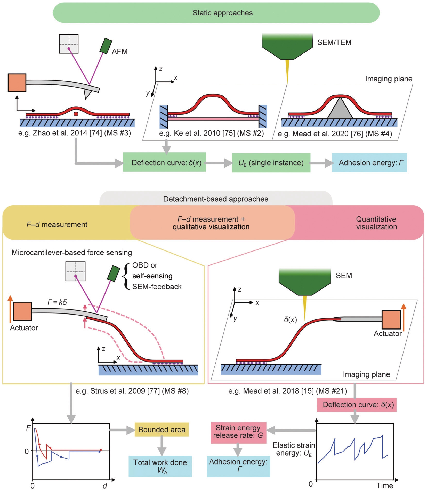
Fig. 3. Diagram of how major 1D adhesion characterization techniques are categorized in this review according to their experimental approach [15,74–77]. Experimental approaches are broadly characterized into static and detachment-based approaches. Detachment-based approaches are sub-categories into F–d measurement, F–d measurement and qualitative visualization, and quantitative visualization approaches. TEM: transmission electron microscopy; F: force; d: distance; OBD: optical beam deflection; k: beam stiffness; δ: deflection; x: distance from adhesion point.
This review focuses on experimental approaches, of which there are a relatively small number of published works. Nevertheless, the observed attachment and detachment behavior, the mechanics of interfacial contact, and the methods used to quantify the interfacial adhesion of 1D materials are supported by an expansive body of theoretical and numerical works. In regard to the mechanics of an interfacial contact, Fischer-Cripps [78] evaluated the deformation associated with pressure induced by two elastic contacting bodies. The Johnson–Kendall–Roberts (JKR) [79] and Derjaguin– Muller–Toporov (DMT) [80] models were subsequently developed to account for adhesion and Hertzian contact, and were found to be most applicable for interfacial component materials with lower and higher elastic moduli, respectively. The Maugis–Dugdale model is valid for intermediate cases using the Tabor parameter [81,82]. Kendall [83] investigated the peeling of elastic thin films, with an analytical solution that is also commonly used to analyze the peeling of NWs and nanotubes. Kendall [83] described the balance that exists between the elastic strain energy and the adhesion energy during peeling, using knowledge of the peel angle and far-field peel force. A review by Gu et al. [84] describes the development of peeling models and their application for quantifying surface adhesion.
The binding energy between CNTs and a variety of nanoscale structures has been theoretically evaluated in a number of studies by considering only vdW interactions. The vdW interactions can be approximated using an analytical continuum model based on the Lennard–Jones (LJ) potential and can be supported by molecular dynamics (MD) simulation [85,86]. The cohesive energy and binding energy between two parallel CNTs, two crossed CNTs, and CNTs/graphene have been theoretically evaluated [87–89]. The binding energy between CNT serpentines and Si, SiO2, and graphite substrates has been theoretically determined, as well as their mechanical stability [90]. When a CNT lies on a substrate, the capacity for vdW forces to induce radial deformation within the CNT has been modeled by MD simulation [91]. Continuum and MD models have also been used to clarify the peeling behavior of CNTs from planar substrates, including the transition from a line contact to a point contact and final detachment [92–96].
The peeling behavior of NWs from planar substrates in humid and non-humid environments has been theoretically investigated by considering vdW and capillary forces in modified Kendall peeling models [97,98]. Capillary forces associated with the liquid bridge that forms at the interface can be approximated using continuum models based on the Young–Laplace equation, the Kelvin equation for a thermodynamic equilibrium [99,100], and the volume equation for non-equilibrium [101]. The vdW interactions under a different peeling configuration were also investigated using a continuum model [102], while vdW interactions between CNTs encapsulated by hollow metallic NWs have been investigated using MD simulation [103].
《3. Static techniques》
3. Static techniques
Static techniques for investigating the interfaces formed by 1D materials have been developed by Chen et al. [104] (MS #1), Ke et al. [75] (MS #2), Zhao et al. [74] (MS #3), and Mead et al. [76] (MS #4). In all four studies, the 1D material under study was ‘‘passively” restrained by its surrounding structure in a way that maintained a partially adhered 1D interface. The method of restraint is referred to here as ‘‘passive” to clarify that the partially formed state of the interface was not or no longer enforced by the controlled movement of a nanomanipulator tip/microcantilever. In each study, the passive restraint(s) enforced a segment of the 1D material(s) to remain detached and deflected, while another segment remained fully adhered.
All four studies considered that the position of the interfacial crack front(s) that accompanies the partially formed interface(s) was dictated by a balance between the elastic strain energy stored in the deflected segment of the 1D material and the adhesion energy of the interface(s) within the vicinity of the crack front(s). To be concise, this concept will hereon be referred to as the ‘‘adhesion–strain energy equilibrium.” Recognizing the existence of this equilibrium permitted these studies to quantify the adhesion energy of the interface by simply equating it to the strain energy stored in the deflected segment of the 1D material. In this way, these studies needed only to use microscopy to observe the elastically deformed shape of the detached segment and the structural geometry (e.g., the cross-sectional dimensions) of the 1D material. Then, with knowledge of the material’s intrinsic elastic properties, the stored strain energy could be quantified using an appropriate analytical or numerical mechanical model.
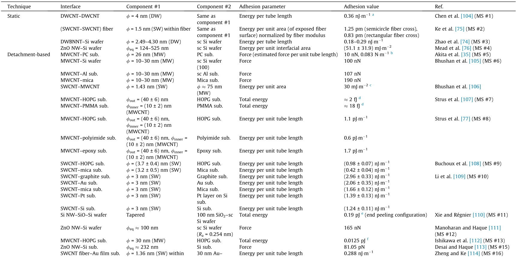
In 2003, Chen et al. [104] (MS #1) experimentally evaluated the 1D interface formed between a pair of CNTs. Their technique exploited a serendipitous event where two CNTs grown from catalyst particles via chemical vapor deposition (CVD) bonded together to form a free-standing bundle. The catalyst particle conveniently restrained the ends of each CNT so that long segments remained separated and then met together to form a junction. The partially delaminated tube–tube interface is shown in Fig. 4(a) [104]. TEM was used to observe the deflection of the detached segment of both CNTs and to determine their diameters/cross-sections. The detached segment of each CNT was treated as an elastic beam, and Timoshenko beam theory was used to evaluate the stored elastic energy. An interfacial adhesion energy per unit tube length of 0.36 nN·m–1 was determined for an interface formed between a pair of double-walled CNTs (DWCNTs). Further details on each interfacial component, as well as the determined adhesion energy values for all experimental characterization techniques discussed in this review, are provided in Table 1 [15,35,74–77,104–116].
Unlike Chen et al. [104], Ke et al. [75] (MS #2) evaluated the adhesive interactions between single-walled CNTs (SWCNTs) within a bundle (hereon simply referred to as CNT bundles) in 2010. The cohesive strength of CNT bundles is critical for their application as structural components and is governed by the adhesive interaction between the individual CNTs that make up the bundle [117,118]. The CNT bundles were first brushed over a TEM grid, causing them to be transferred, aligned, and suspended over the windows of the grid. In some instances, the large axial force applied during the brushing process caused fibers within a bundle to slide past each other, which could result in a partially separated bundle consisting of a buckled fiber segment and a straight fiber segment. TEM was used to observe the deflection shape of the bundle, as shown in Fig. 4(b) [75]. A computational elastica model was developed, and the approximated deflection shape was found to be in good agreement with the TEM observations. The model also computed an adhesion energy parameter based on the delamination moment, building upon previous work by Goussev et al. [119]. Further details regarding the elastica model are provided in Table 2 [15,74–77,102,107–109,113–115,117,120– 125], which summarizes the key mechanical deformation models explored in this review.
《Fig. 4》
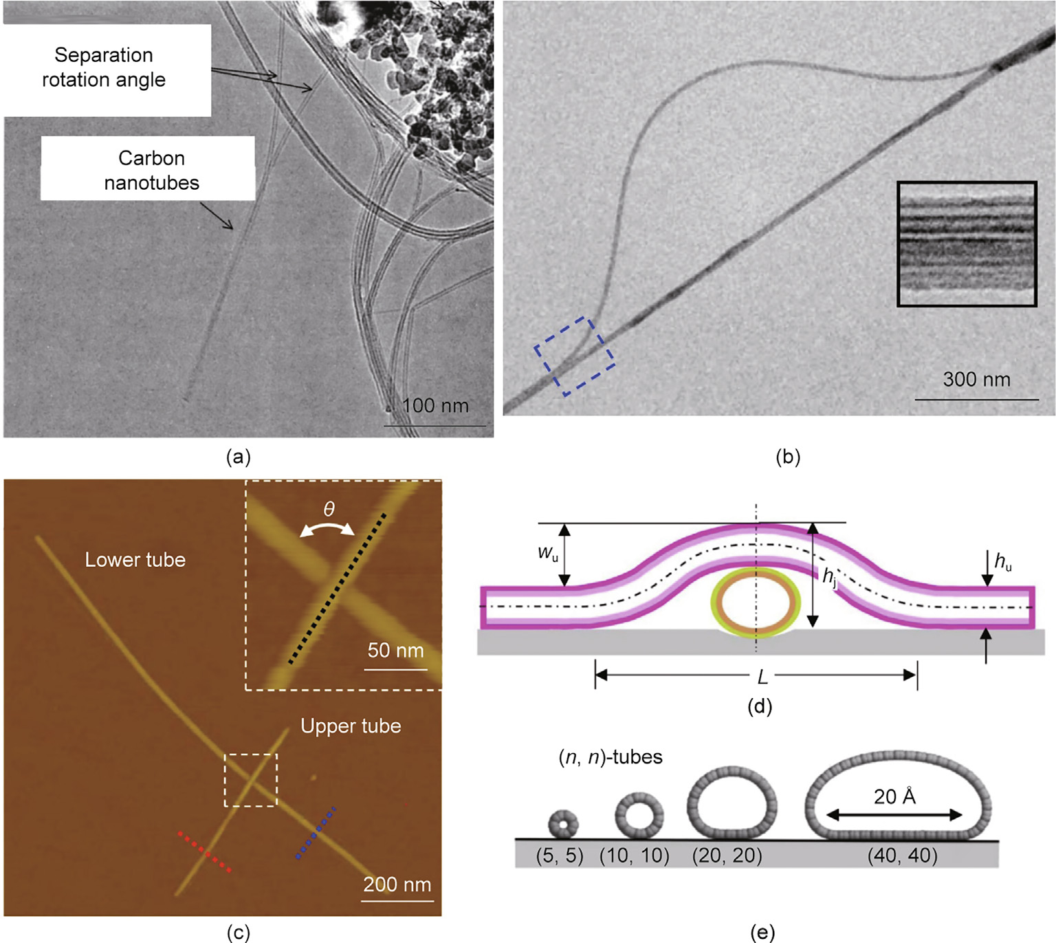
Fig. 4. (a) TEM micrograph of CNT–CNT junction, used by Chen et al. [104] (MS #1) to conduct a static assessment of their interfacial adhesion. (b) TEM micrograph of a suspended CNT bundle with a partially delaminated and buckled CNT fiber. Evaluation of the buckled shape of the CNT fiber by Ke at al. [75] (MS #2) permitted a static assessment of the binding energy between individual CNTs. (c, d) Zhao et al. [74] (MS #3) carried out interfacial adhesion assessment of BNNTs on a Si substrate by the AFM examination of formed cross-junctions: (c) AFM micrograph with inset showing the center of the cross-junction; (d) diagram of the cross-junction whereby the lower tube induces partial separation of the upper tube. (e) MD-simulated radial compression of various single-walled CNTs (SWCNTs) with different diameters on graphite, induced by vdW interactions. θ: angle of cross-junction; wu: central deflection of the upper tube; hj: total height of the crossed tubes at the junction; hu: height of the upper tube; L: distance between two delamination fronts; (n, n): lattice vectors. (a) Reproduced from Ref. [104] with permission; (b) reproduced from Ref. [75] with permission; (c, d) reproduced from Ref. [74] with permission; (e) reproduced from Ref. [91] with permission.
Using the delamination of a CNT bundle to evaluate the interfacial interactions between individual CNTs within the bundle comes with some challenges. To be specific, the exact number of CNTs and their assembly configuration within the fiber are difficult to precisely determine by means of TEM, due to overlapping effects. This issue introduces uncertainty when computing the bending stiffness of the fiber and the area of the newly formed interface. Recognizing this, Ke et al. [75] presented normalized adhesion energies for bundles with different cross-sections (Table 1). In the quasistatic techniques that will be presented later (i.e., Zheng and Ke [114] (MS #16), Ke et al. [115] (MS #17), and Chen et al. [125] (MS #18)), the same uncertainties persist regarding the number and configuration of CNTs within a bundle.
《Table 1》
Table 1 Summary of experimentally determined interfacial adhesion properties for 1D materials.
Commercial Si wafers or the etched surfaces of an AFM cantilever can be used as Si substrates. ‘‘Si wafer” denotes that a wafer is used. ‘‘Si sub.” denotes that etched Si surface or similar is used. SW: single-walled; DW: doublewalled; MW: multi-walled; SWCNT: single-walled CNT; DWCNT: double-walled CNT; DWBNNT: double-walled BNNT; MWCNT: multi-walled CNT; PC: polycarbonate; HOPG: highly ordered pyrolytic graphite; sub.: substrate; sc: single crystal; Φ: diameter; Φeq: equivalent diameter; Φout: outer diameter; Φinner: inner diameter; Ra: surface roughness.
a Presented in different units from the original units, UA = 0.036 nN (1 nN = 1 nJ·m–2), where UA is the work of adhesion.
b Calculated from original values of Ftotal = 10 nN, Ladh = 120 nm, where Ftotal, Ladh are total adhesive force and adhered length, FA = Ftotal/Ladh.
c Presented in different units from the original units UA = 0.03 N·m–1 (1 N·m–1 = 1000 mJ·m–2).
d Approximate values extracted from histograms presented in cited article
e Converted from original units presented as UA = 1185 keV (1 eV = 1.602176634 × 10⁻¹⁹ J).
f Converted from original units presented as UA = 78 keV.
《Table 2》
Table 2 Key mechanical deformation models.


In 2014, Zhao et al. [74] evaluated the interface formed between BNNTs and a Si substrate by examining the formation of crossjunctions. Cross-junctions formed by CNTs had also been examined previously [126,127]. A dispersion containing BNNTs was deposited on a Si substrate via spin coating. Occasionally, a tube was found to have been deposited over another, forming a crossjunction where the lower tube induced partial separation of the upper tube from the substrate, as respectively shown in the AFM micrograph as well as diagrammatically in Figs. 4(c) and (d) [74]. AFM was used to measure the height profile along the length of the partially suspended tube. The longitudinal height measurement permitted the position of the interfacial crack front and the contact point between the upper and lower tubes to be determined, as well as the deflected shape of the suspended tube segment. Radial compression of the lower tube occurred as a result of the contact between the upper and lower tubes, and was accounted for. The radial compression of SWCNTs with different diameters is shown diagrammatically in Fig. 4(e) [91]. The diameter of each tube was also obtained by measuring their height using AFM. The wall number of each tube was determined by compressing an adhered segment of the tube with the AFM tip and measuring the tube height once in an entirely compressed state [128]. The deflected shape of the suspended segment of the upper tube was assumed to be symmetric about its contact point with the lower tube. Therefore, to evaluate the stored strain energy, each side of the suspended region was treated as an Euler–Bernoulli fixed– fixed beam experiencing a pure-bending loading condition [74,123]. Further details regarding the model are provided in Table 2. An interfacial adhesion energy per unit tube length of 0.18–0.29 nN·m–1 was determined for the interface between double-walled BNNTs (DWBNNTs) and the Si wafer (Table 1).
While the other static techniques investigated NTs, Mead et al. [76] presented a static approach in 2020 for studying NW interfaces. A wedge structure, fabricated by focused ion beam (FIB) milling, was fastened to a Si wafer via electron-beam-induced deposition (EBiD) Pt. ZnO NWs were draped over the wedge using a well-established OM-based NM-assisted pick-and-place strategy [129,130] in order to form an NW ‘‘arch,” as shown in Fig. 5(a) [76]. The suspended regions of the NW arch exhibited fringe patterns, as shown in Fig. 5(b) [76], and subsequent interferometric analysis was used to construct the NW’s deflection profile. The irregular axisymmetric hexagonal cross-section and the tapering along the length of each NW was defined by combining SEM and AFM measurement after adhesion testing. An Euler–Bernoulli fixed–fixed beam model (Table 2) that assumed pure bending loading conditions provided deflection profiles that matched the observations, and was used to compute the total stored strain energy [123]. An interfacial adhesion energy of (51.1 ± 31.9) mJ·m–2 was obtained for the interfaces formed between the ZnO NWs and the Si substrate (Table 1).
Effective characterization techniques should facilitate the rapid examination of a large population of samples in order to compute statistically significant adhesion energy parameters. Methodical sample examination is particularly important for 1D materials, as there is not yet a complete consensus on whether the adhesion energy exhibited by a 1D material is diameter dependent (or shell number dependent, with respect to NTs) or is simply an artefact of a poorly defined interfacial area. The techniques developed by Chen et al. [104] and Zhao et al. [74] rely on the chance occurrence of their respective 1D materials forming a partially delaminated state. Zhao et al. [74] evaluated 12 separate cross-junctions formed from BNNTs of varying diameters, which indicates that the spincoating method frequently produced near-perpendicular crossjunctions. Chen et al. [104] evaluated only a single tube–tube junction; therefore, it can be surmised that the identification of junctions with perpendicular alignment to the TEM column may occur less frequently. In contrast to simply exploiting the selfformation of partially delaminated interfaces, Mead et al. [76] relied on the deliberate control of an NM tip to form NW arches. In addition to enabling the examination of 11 different NW samples, NM allowed the authors to examine how the interfacial crack front responded when further constraint was introduced to the system. This was done by momentarily perturbing the suspended segment of the NW. As shown in Fig. 5(b), the stationary crack front (parts (i) and (ii)) momentarily recedes as additional restraint is induced by the NM tip (parts (iii) and (iv)) and then the crack front extends to return to its original position once the NM tip is removed (parts (v) and (vi)). This demonstration provided direct evidence that the position of the crack front was indeed dictated by an adhesion–strain energy equilibrium.
《Fig. 5》
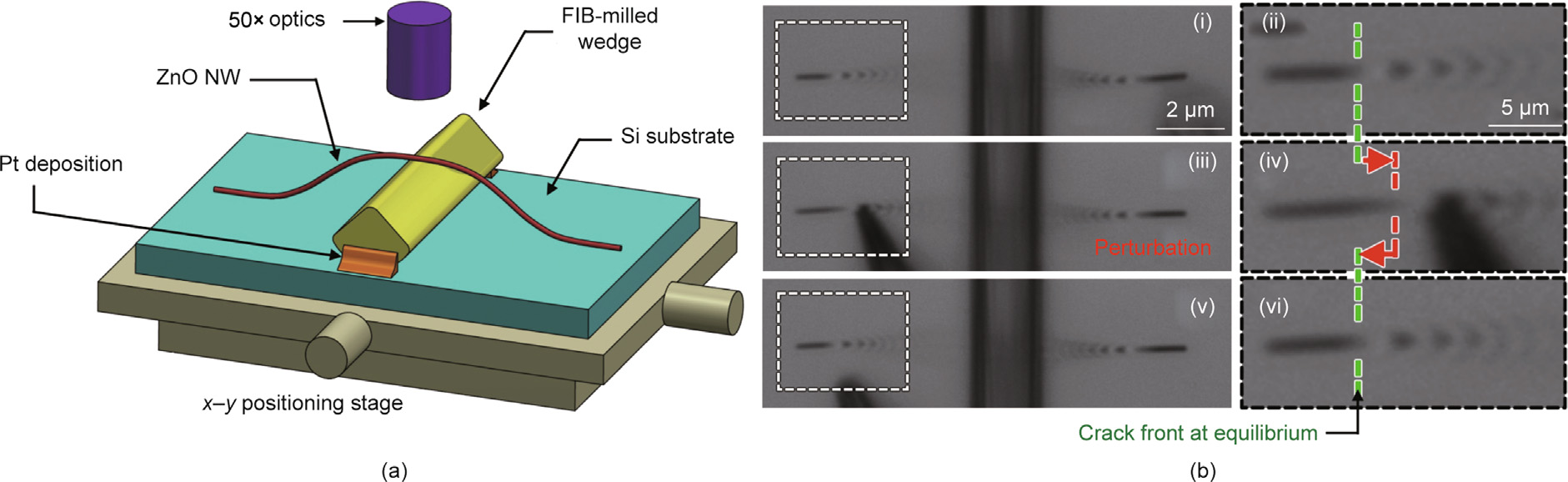
Fig. 5. An NW ‘‘arch” method for characterizing NW–substrate adhesion by Mead et al. [76] (MS #4). (a) Diagram of a ZnO NW draped over a FIB-milled wedge on a Si substrate forming a NW arch with a partially delaminated interface. (b) A series of optical micrographs showing the state of the NW arch during equilibrium, as well as when a perturbation is applied by an NM tip. The fringe patterns indicate the position of the crack front. The NW arch is at equilibrium in part (i) and a corresponding inset is provided in part (ii). The crack front recedes when strain is induced in the suspended segment of the NW in part (iii) and a corresponding inset is provided in part (iv). The crack extends to return to its original position when the NM tip is removed in parts (v) and (vi). Reproduced from Ref. [76] with permission.
The test environment and the prior environmental history experienced by a 1D interface can irreversibly alter its interfacial interactions and therefore permanently change its adhesive behavior [15]. Static techniques can hence be limited by the fact that the observed position of the crack front may actually be an artefact of previous environmental conditions and therefore may no longer correspond to an equilibrium state. In such a case, the crack front may no longer be capable of extending or receding to establish a renewed equilibrium when new constraints are applied or under new environmental conditions. The perturbation demonstration carried out by Mead et al. [76] is therefore an effective method of confirming that a partially delaminated interface continues to correspond to a minimum energy state. The CNT–CNT junction studied by Chen et al. [104] was formed in an Ar furnace at temperatures as high as 900 °C [131]. Any defects present in the tube lattice may have permitted chemical bonding to occur between tubes, potentially anchoring the crack front and preventing it from establishing a new equilibrium once placed in an ambient environment. Furthermore, CNT examination was conducted in a vacuum environment, irradiated by a 200 kV electron beam (EB). Aside from the moisture-free environment not reflecting real device conditions, knock-on damage caused by the EB may have led to defects or chemical bonding at the interface of interest [132]. The dispersion of the BNNTs examined by Zhao et al. [74] was achieved by dispersing them in a solution of deionized water and an ionic surfactant, as described by the group’s previous work [133]. Once deposited on the Si wafer, the solution was rinsed with further deionized water and air dried. During air drying, any remaining surfactant—as well as any existing dust, debris, or absorbed atmospheric contaminates—could potentially be drawn into the meniscus at the BNNT–substrate interfaces, producing an interfacial residue. Potential evidence of such a residue can be observed on the substrate in the top-left region of the AFM map in Fig. 4(b); exposure of the substrate surface that once formed the interface may be a consequence of the scanning AFM tip shifting the end of the weakly adhered BNNT. The existence of such a residue can potentially alter interfacial interactions and hence alter the adhesive properties. As testing can be conducted in an air environment, OM- and AFM-based examinations have a clear advantage over TEM in regard to ensuring that the observed adhesive behavior is analogous to in-device behavior.
All four static approaches assume that their 1D materials experienced a pure-bending loading condition. The approaches carried out using TEM and OM also assume that the induced deflection occurs entirely within the imaging plane. If the longitudinal axis of a 1D structure is in fact misaligned with respect to the imaging plane, then some deflection will also occur out-of-plane. The observed deflection shape will therefore be a projection of the real deflection profile onto the imaging plane. Similarly, unintentional torsional and/or shear forces applied to a 1D structure will alter its real deflection shape. The abovementioned assumptions can be verified by comparing the deflection curve predicted by an idealized mechanical model to the experimentally observed curve. TEM examination is associated with an extremely large depth of field; therefore, any out-of-plane deflection of a 1D structure—such as the CNT junction examined by Chen et al. [104]—cannot be easily detected. In contrast, OM examination as utilized by Mead et al. [76] is associated with a very small depth of field which depends on the selected objective lens. Consequently, a segment of an NW that significantly deflects out-of-plane will appear blurry. A poorly aligned 1D material can also provide a projection with a shortened axial length and therefore a deflection shape with exaggerated curvature, leading to an overestimation of the stored strain energy and therefore also the adhesion energy. Chen et al. [104] used a single separation distance and angle measurement at a point along the deflected CNT segments to define their deflection shape. Similarly, Zhao et al. [74] measured a single maximum deflection and total length parameter from the suspended segments of the upper tube. In this way, the deflection profiles along the entire length of the suspended segments were not evaluated and therefore do not permit verification of the pure-bending loading condition assumption. Mead et al. [76] obtained numerous deflection coordinates along the suspended length of each NW arch by evaluating the maxima and minima of the exhibited fringe pattern. Fitting the pure-bending mechanical model to the deflection coordinates of a typical arch provided a coefficient of regression of 0.9994, verifying the applicability of the utilized pure-bending model. However, while OM-based interferometry was shown to be effective for measuring the deflection of NWs with effective diameters down to 124 nm, the resolution limit of the readout strategy may prevent the detection of NWs with significantly smaller diameters. The detection of individual NTs via the applied OM strategy is not feasible, as they are too small to interact with light and therefore must rely on the higher resolution capabilities of either TEM or AFM.
Static techniques evaluate a 1D interface while in a single state—when the peel front remains at a single location—and are therefore, by nature, unable to probe the entire length of the interface. Thus, such techniques cannot detect whether the adhesive properties of an interface change along its length. This limitation becomes evident when considering the results obtained by Mead et al. [76], whose examination of 11 NWs provided a nominal adhesion energy value with a relative standard deviation of ±62%. The authors recognized that the deviation lay outside of the bounds of uncertainty associated with the experimental setup and hypothesized that the deviation could be attributed to a nonuniform interfacial condition along the length of an NW. More specifically, it was concluded that the NW formed contact with the substrate in discrete locations. The nature of this interfacial condition and its implications for evaluating the adhesion of 1D interfaces will be discussed in detail in Section 5. Nevertheless, evidence of a nonuniform condition being present at 1D interfaces highlights the limitations of probing using a static approach. Quasi-static techniques that can probe the entire length of a 1D interface are therefore better suited for an adhesion energy assessment with improved repeatability and statistical significance.
《4. Detachment-based techniques》
4. Detachment-based techniques
《4.1. Force–distance measurement》
4.1. Force–distance measurement
The first experimental works to examine the adhesive behavior of 1D materials during a detachment process arose from an interest in exploiting CNTs as tips for enhanced AFM microcantilever probes [134]. CNTs were adhered by one end to the pyramidal tip of a commercial microcantilever probe, so that it remained cantilevered out from the probe, with its longitudinal axis aligned perpendicular to that of the main microcantilever beam. Such assembled probes will hereon be referred to as ‘‘CNTmicrocantilever probes.” The CNT component of such probes provides a highly robust and functionalizable tip capable of high resolution imaging of high-aspect-ratio samples [36,135]. The first research activities in this area typically relied on the forcesensing capability of a commercial AFM to explore the adhesive behavior of CNTs. Specifically, during the approach and retraction of a CNT tip from the surface of a substrate, the normal attractive and repulsive forces between the tip and substrate induce vertical deflection in the main microcantilever beam. This deflection is then commonly detected using the optical beam deflection (OBD) method and is proportional to the normal force via the spring constant of the microcantilever. Such experimental setups are therefore essentially ‘‘blind” in regard to directly observing the deformed state of a 1D material during interface formation and detachment. The deformation behavior of the CNT can therefore only be deduced from mechanical models with a corresponding set of assumptions.
In 2000, Akita et al. [35] (MS #5) measured the adhesive force between a CNT-microcantilever probe and a polycarbonate (PC) surface. The CNT-microcantilever probe was assembled using EBiD amorphous carbon inside an SEM [36]. The force–displacement response of the CNT was first calibrated by detaching it from the surface of a highly compliant microcantilever. To do this, the free end of the CNT was brought into line contact with the planar surface of the compliant microcantilever, as shown in Fig. 6(a) [35]. The stiff cantilever was then displaced horizontally to the left, deflecting and then buckling the CNT. Deflection of the compliant cantilever with the known spring constant was observed via SEM over the duration of the test, which permitted a force–displacement relationship to be obtained. This process was repeated for the same CNT at different contact lengths, and the corresponding force constants were obtained. The CNT-microcantilever probe was then used to carry out tapping-mode scanning of the surface of a PC disc containing pits. When scanning over a pit, the free end of the CNT would come into contact with the side-face of the pit such that a segment of its free end was assumed to form a line contact, as shown in Fig. 6(b) [35]. The CNT was found to detach from the side-face only after the probe had moved to a specific horizontal distance away from the face. The pre-calibrated force constant of the CNT was then used to deduce an adhesive pull-off force of 10 nN (Table 1). Akita et al. [35] concluded that continuum mechanics theory for isotropic materials remains applicable for interpreting CNT behavior in such tests.
《Fig. 6》
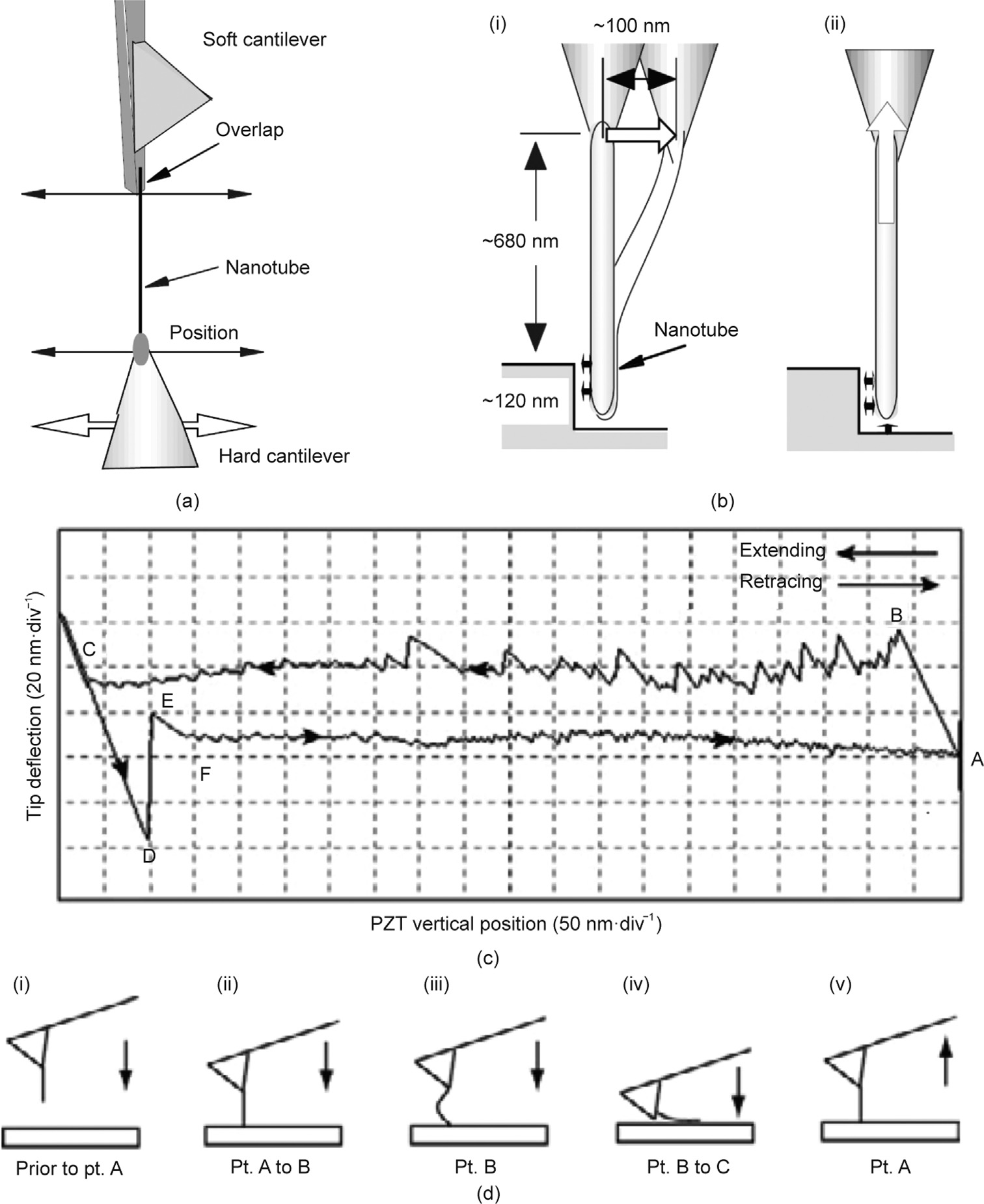
Fig. 6. (a, b) Vertically aligned CNT-microcantilever probe in contact with a sidewall present on a sample surface by Akita et al. [35] (MS #5): (a) schematic of the experimental configuration used for the force–deflection calibration of a CNT; (b) lateral movement of the CNT-microcantilever leading to the contact and detachment of the CNT tip from the sidewall. (c, d) Attachment–detachment of a vertically oriented CNT-microcantilever probe from a planar substrate by Bhushan et al. [105] (MS #6): (c) uncalibrated force–distance approach–retraction curve; (d) each stage of the approach–retraction procedure is (i) probe lowered toward the surface, (ii) contact of the end of the CNT with the substrate, (iii) Euler buckling of the CNT, (iv) sliding point contact of the CNT’s end, potentially forming a line contact, and (v) retraction of the probe. nm·div–1 : nanometers per division on the graph; PZT: piezoelectric transducer; A–F: specific points on the force–distance curve; pt.: point. (a, b) Reproduced from Ref. [35] with permission; (c, d) reproduced from Ref. [105] with permission.
Akita et al. [35] did not directly observe the deflected shape of the CNT during interaction with the PC disc. The application of a calibrated force constant assumes that the deformation configuration of the CNT during the tapping-mode scanning matches that of the calibration experiment. Full conformation of the CNT to the 120 nm deep sidewall of the pit must also be assumed when defining the effective length of the CNT. Uncertainty regarding these assumptions was introduced into the calculated adhesion force. The calculated adhesion force was specific to the detachment configuration, the interfacial adhesion area (length of contact), and the diameter and shell number of the CNT, making it difficult to compare this force with other experimental results. Assuming that the adhered length of the CNT corresponded to the full height of the side-face, an adhesive force per adhered length of 0.083 Nm1 can be computed (Table 1).
In 2004, Chen et al. [135] also studied the adhesive behavior of a CNT-microcantilever probe in order to better define tip-induced broadening effects during tapping-mode imaging. A case in which the end of a vertically oriented CNT formed a single-point contact with the horizontal surface of a substrate, prior to buckling, was considered. Conformation of the CNT—that is, of the formation of a 1D interface—was not considered. In 2005, Dietzel et al. [136] recognized that further compression of the CNT tip of a CNTmicrocantilever probe resulted in single-point contact with a substrate, followed by buckling of the CNT and sliding of its end along the substrate surface. By evaluating the adhesion hysteresis present in the frequency shift and the damping of the microcantilever during amplitude modulation, the researchers recognized that a completely different adhesive contact could occur, but did not elucidate as to whether a 1D interface had been formed. In 2005, Strus et al. [137] investigated the interaction between a CNTmicrocantilever probe and textured substrates using dynamic force microscopy.
In 2008, Bhushan et al. [105] (MS #6) produced CNTmicrocantilever probes with the CNT aligned perpendicularly to the main microcantilever beam, similar to the probe configuration used by Akita et al. [35]. CNT transfer was achieved by first applying a bias voltage between a donator tip and the final microcantilever tip to improve the alignment, followed by physical welding to fasten the CNT to the microcantilever and, finally, the use of Joule heating to detach the CNT from the donator tip. The CNT-microcantilever probe was then installed and actuated in a commercial AFM to bring the multi-walled CNT (MWCNT) in and out of contact with Si, Al, and mica substrates. The microcantilever deflection was recorded simultaneously with the vertical position of the piezo-positioner, permitting an ‘‘uncalibrated” force– distance curve to be obtained, as shown in Fig. 6(c) [105]. The force–distance curve is referred to as uncalibrated here because the y-axis is given in terms of the microcantilever deflection, not in terms of force. Features on the force–distance curve were deduced to correspond to the changing deformation configurations of the CNT during approach and retraction, with each proposed configuration step diagrammatically illustrated in Fig. 6(d) [105]. In Fig. 6(c), point A corresponds to the initial contact between the end of the CNT and the substrate (stage (ii) in Fig. 6(d)). Between points A and B, a linear relationship is observed between the microcantilever deflection and the piezo-position; this is due to the CNT remaining undeformed, with only deflection of the main cantilever occurring. It is only once the applied force reaches the critical buckling force of the CNT at point B that the CNT begins to buckle (stage (iii) in Fig. 6(d)). Buckling can initially be considered to occur in a manner such that the CNT’s end remains in point contact with the substrate, as previous described by Chen et al. [135]. However, after point B, the force–distance curve shows a series of sawtooth features that follow a relatively constant microcantilever deflection over a long piezo-displacement range until the Si tip of the microcantilever snaps into contact with the substrate at point C. Bhushan et al. [105] ascribes this sawtooth behavior to a competition between the buckling of the CNT (stage (iii) in Fig. 6(d)) and the sliding of its end along the substrate (stage (iv) in Fig. 6(d)). This process is dictated by both adhesion and friction. After point C, the CNT can be considered to be fully buckled and can deflect no further. Therefore, further lowering by the piezopositioner only serves to deflect the Si cantilever and hence provides a linear force–displacement relationship again. Upon retraction, the Si cantilever snaps out from point D to E, and another sawtooth region is observed until the detachment of the CNT at point A. It is important to note that the microcantilever deflection during the approach and retraction was dictated not only by its spring stiffness but also the stiffness of the CNT. Consequently, the relation between the applied force and the microcantilever deflection was not always linear; rather, it also depended nonlinearly on the CNT deformation configuration. The adhesive force associated with the attachment and detachment of the CNTmicrocantilever probe was calculated (Table 1).
Bhushan et al. [105] noted that the calculated adhesion force consists of contributions from both the CNT and the Si microcantilever tip. For example, during the snap-out of the Si tip (between points D and E), a portion of the CNT may also be detached, and this cannot be isolated in the corresponding force–distance curve. Furthermore, the vertically aligned CNT can only conform to the substrate via sliding, so sliding and buckling occur simultaneously between points B and C. Consequently, the forces associated with adhesion cannot be separated from the friction force. The forces associated with the approach were much higher than those of the retraction, and was expected to be due to the significant contribution of friction during the approach. This result shows that a vertically oriented 1D material is not particularly suitable for characterizing adhesion in isolation from friction.
With the specific aim of characterizing the adhesion of 1D materials, Strus et al. [77,107] assembled CNT-microcantilever probes in 2008 (MS #7) and 2009 (MS #8) with an alternative configuration that permitted the CNT to be controllably peeled off the substrate without sliding. MWCNTs were attached to tipless microcantilevers such that the longitudinal axis of the CNTs was oriented parallel to the microcantilever beam axes, as shown diagrammatically and by the SEM micrograph in Figs. 7(a) and (b) [77,107], respectively. This probe configuration was distinct from that utilized by Bhushan et al. [105] and Akita et al. [35]. The transfer and fastening of the NTs was achieved by the application of a bias voltage [138], similar to that performed by Bhushan et al. [105]. To study the adhesive behavior of NTs on various substrates, approach–retraction tests were conducted using a commercial AFM system, whereby the NT was oriented near parallel to the substrate. Theoretical and experimental peeling force–distance curves for both the approach and the attraction stages of testing are shown in Figs. 7(c-i) and (d) [77], respectively. As the AFM-based technique could not directly observe the deformed shape of the CNT, interpretation of the features on an experimental force– distance curve was conducted through a comparison to theoretical curves derived from an elastica model (Table 2) [102].
The theoretical force–distance curves (Fig. 7(c-i)) clarify that, with the CNT oriented parallel to the substrate surface, multiple deflection profiles are simultaneously possible. To be specific, the CNT can exhibit an S-shaped (Fig. 7(c-ii)) or arc-shaped deflection profile (Fig. 7(c-iii)). The black curve in Fig. 7(c-i) indicates deflection solutions whereby the NT can adopt a minimum energy state. The red dashed line demarcates the approach curve, and the blue line demarcates the retraction curve. Experimentally, the approach and retraction occurred at a constant rate of piezo-displacement; therefore, not all segments of the minimum energy curve could be accessed. This situation is illustrated as discontinuities on the theoretical approach and retraction curves, where the CNT suddenly switches between deflection states. During retraction, the CNT is predicted to adopt a line-contact interface with the substrate and to initially deflect in an S-shape (pink dashed line in Fig. 7(c-i)). Next, the CNT is predicted to discontinuously transition to an arch-shaped deflection profile, where it maintains a singlepoint contact with the substrate. The model further deduces that, for NTs with small aspect ratios, the work done by the retracting microcantilever during the S-shape peeling is primarily associated with a change in the interfacial energy of the system (i.e., extension of the NT peel front). In contrast, during the arc-shape deflection of the CNT, the work done is primarily associated with a change in strain energy (i.e., further buckling of the NT). The latter prediction is intuitive, considering that the interfacial state remains as a point contact (i.e., does not grow or recede) until the final detachment of the CNT.
The experimentally obtained force–displacement curves exhibited the same features as the theoretical curves. A clear transition from S-shape peeling to arc-shape deflection was defined by a sudden drop in load, and point contact was associated with a gradually increasing load until detachment (Fig. 7(d)). There was one difference, however: At the end of the approach and at the start of the retraction, the snap-in and snap-out of the microcantilever produced clear features on the load–displacement curve, similar to those observed by Bhushan et al. [105]. During peeling, the system was considered to be in a quasi-static equilibrium, whereby the rate of strain energy released from the NT was equal to the adhesion energy of the interface. Therefore, the total adhesion energy of the interfaces formed between the MWCNT and a respective substrate was quantified by summing the area bound only by the segment of the retraction curve associated with S-shape peeling. It was therefore necessary to clearly define the segment of the retraction curve associated with microcantilever snap-out and disregard it (this segment can be observed in the inset in Fig. 7(d)). The green shaded area in Fig. 7(d) shows the region used to quantify the interfacial adhesion energy. Nominal total adhesion energy values were obtained for interfaces between MWCNTs and highly ordered pyrolytic graphite (HOPG), polyimide, and epoxy, as provided in Fig. 7(e) and Table 1.
《Fig. 7》

Fig. 7. (a) MWCNT peeling from planar substrates via a parallel-aligned CNT-microcantilever probe by Strus et al. [107] (MS #7). Schematic shows the S-shaped peeling of the MWCNT from a planar substrate. (b–e) Refinement of the CNT peeling technique for adhesion energy assessment by Strus et al. [77] (MS #8). (b) SEM micrograph of MWCNT tip fastened to the microcantilever. (c-i) Theoretically derived force–displacement curve for the approach–retraction of the MWCNT from a substrate (cantilever attachment– detachment event is not included). Regions where S-shaped peeling of a line contact occurs are filled in green. The region where arc-shaped detachment via a point contact occurs is filled in orange. (c-ii, c-iii) Diagrammatic illustration of (c-ii) line contact and (c-iii) point contact. (d) Force–displacement curve experimentally obtained by peeling a CNT from a HOPG substrate. Green fill indicates the region where S-shaped peeling is expected to occur, and is used to quantify the total adhesion energy. (e) Histogram showing the total adhesion energy distribution obtained from peeling on graphite, polyimide, and epoxy substrates. P: force applied by microcantilever; Kcant: microcantilever spring stiffness; zr : piezo displacement; δ: total deflection of CNT;  : deflection of microcantilever; s: arc-length/distance from peeling point along longitudinal axis of CNT; x: distance from peeling point along the x-axis; θ: slope of CNT/angle between CNT longitudinal axis and the x-axis; LCNT and L: length of CNT projected along the x-axis;
  : CNT–substrate interaction force per unit length; c: constant representing the slope of the force–displacement curve; # of tests: number of tests. (a) Reproduced from Ref. [107] with permission; (b–e) reproduced from Ref. [77] with permission.
The well-defined and repeatable force–distance curves obtained by Strus et al. [77] contrast with the stick–slip sliding behavior exhibited during the approach and retraction of the CNTmicrocantilever probe investigated by Bhushan et al. [105] (see sawtooth pattern in Fig. 6(c)). These results show that CNTmicrocantilever probes with a parallel-aligned CNT tip are ideal for achieving controllable non-sliding conformal S-shape peeling behavior and are therefore well-suited for the fundamental characterization of 1D interfaces. The approach–retraction tests performed by Strus et al. [77] were sufficiently straightforward to implement, and the probes were adequately robust, permitting hundreds of peeling measurements to be conducted prior to probe failure. This permitted nominal total adhesion energies to be obtained with high statistical significance.
Nevertheless, as per the previous AFM-based techniques, Strus et al. [77] were unable to directly observe the deformed shape of the CNT during testing, which prevented them from verifying that the CNT was precisely aligned with the substrate. Furthermore, the contact length of the CNT at a given moment during S-shape peeling could not be determined, preventing an adhesion energy per unit tube length value from being obtained. Using the assumption that the entire cantilevered length of a CNT was able to form contact with the substrate, Strus et al. [77] provided a lower bound estimation of the adhesion energy per unit tube length, as given in Table 1, and noted the limitations of this assumption. More specifically, during testing, a segment of a CNT is expected to already detach during the snap-out of the Si microcantilever, countering the above assumption. Strus et al. [77] also emphasized that multiple discontinuities were commonly observed in the retraction curves. These additional discontinuities may have occurred due to the CNT imperfectly conforming to the substrate and may originate from defects or asperities present on the surface of either the CNT or the substrate. The distribution of such asperities can be seen along the MWCNT in Fig. 7(b). Multiple discontinuities in the force–displacement curves could also generate uncertainty regarding when a CNT transitions from S-shaped peeling to arc-shaped deflection. Imperfect conformation may also help to explain why the approximated adhesion energy per unit area value obtained for MWCNTs on HOPG substrates was two orders of magnitude lower than that obtained between two SWCNTs, as presented by Chen et al. [104] above.
In 2011, Buchoux et al. [108] (MS #9) and, in 2015, Li et al. [109] (MS #10) applied their custom-built interferometric-based AFM facility to investigating the peeling of SWCNTs with a much smaller diameter than that of previously investigated CNTs. It can be generally assumed that SWCNTs are too small (diameter (Φ) = 3.7 nm for an SWCNT [108], compared with Φ = 40.0 nm for an MWCNT [107]) for nanohandling-based methods to be used to fabricate a CNT-microcantilever probe. In line with this assumption, the CNTs were instead grown directly on the tip of the microcantilever using CVD [139]. The interferometry-based AFM (an alternative readout method to the OBD approach) was capable of providing a time–frequency analysis of the microcantilever deflection during the approach and retraction process, even when the CNT was in contact with the substrate [140]. The dynamic stiffness of the contacting CNT could therefore be evaluated, allowing its intrinsic mechanical properties to be defined with higher accuracy. Each study used a different test configuration: respectively focusing on the peeling of cantilevered CNTs [108] and CNT loops [109] from various substrates. When using the cantilevered CNT configuration, the longitudinal axis of the CNT was oriented at an angle with the substrate, unlike Strus et al.’s [77] peeling force spectroscopy. As previously discussed, Bhushan et al. [105] (MS #6) had observed that CNTs under a similar configuration had tended to slide along the substrate during conformation. In contrast, Buchoux et al. [108] considered that, as the tested CNTs were particularly long, deflection of the suspended segment occurred preferentially over sliding along the substrate. The deformed shape of the CNT during peeling was predicted using an elastica model (Table 2) [98], demonstrating that the bent shape of the CNT in the vicinity of the peel front remained relatively stable and corresponded to a plateau in the measured peel force. The interfacial adhesion energy was equated to the strain energy stored within this local segment, simply defined by a local radius of curvature. During the detachment of the CNT loop investigated by Li et al. [109], two independent peel fronts tended to form. The interfacial adhesion per unit of tube length was obtained for substrates of graphite, HOPG, Au, mica, Pt, and Si, as presented in Table 1.
The detachment-based techniques described thus far demonstrate the powerful capability of AFM to carry out the approach and retraction of CNTs from a substrate in a controlled manner with force feedback. However, AFM has not yet been routinely utilized for the study of NW adhesion. This can be partially attributed to the additional experimental difficulties that are introduced by NWs having significantly higher bending stiffness values and surface areas in comparison with NTs. More specifically, NW handling and fastening during probe assembly and NW actuation during testing are more difficult to realize in comparison to applying the same processes to NTs. For example, due to the higher bending stiffness of an NW, a misaligned application of force to the NW by an NM during nanohandling can lead to the NW being ‘‘flicked away” (i.e., the dynamic release of strain energy in an NW can overcome the adhesion energy binding it to a surface, propelling it away) before it can be properly fastened during probe assembly. NWs are also not as easily cut; hence, the Joule heating approach exploited by Bhushan et al. [105] (MS #6) and Strus et al. [77] (MS #7) to separate CNTs as part of probe assembly cannot be applied here. Furthermore, the larger surface area of an NW facilitates much higher adhesion forces during testing. This requires the connection between the NW and the microcantilever or actuator to be very secure to ensure failure does not occur during retraction. Hence, NW fastening typically requires the use of a gas injection system (GIS) to deposit robust materials such as EBiD Pt or W. The presence of larger adhesive forces also requires significantly larger actuator displacements to achieve detachment during testing. Such displacements can easily exceed the typical displacement range of the piezopositioner of a commercial AFM (~3 μm).
In 2010, Xie and Régnier [110] (MS #11) developed a dualprobe AFM-based nanotweezer facility that allowed NWs to be peeled directly off a substrate for adhesion characterization. The facility consisted of two separately actuated force-sensing microcantilevers with oppositely facing sharp visible tips that could be brought in contact together through coordinated movement [141]. Uniquely, the technique relied on gripping the NW of interest in situ. In this way, a single experimental configuration was used to locate an NW lying on a substrate, grasp it, and then peel it off. Hence, a separate experimental configuration to first fasten the NW to a microcantilever was not required. Si NWs deposited on a 300 nm SiO–Si substrate were first located by means of AFM scanning with a single microcantilever. To conduct peeling, both microcantilever tips were then brought into contact with the substrate on either side of an NW and actuated to apply a compressive load to the NW, ensuring a secure grasp. The NW could be grasped either at one end, as shown in Fig. 8(a) [110], or at its center; these configurations will hereon be referred to as ‘‘end point” and ‘‘center point” peeling, respectively. Once grasped, the NWs were peeled from the substrate by lifting the cantilevers, and the corresponding cantilever deflection was recorded in order to produce a force– displacement curve, as shown in Fig. 8(b) [110]. End-point and center-point peeling were theorized to form the deflection shapes shown in Figs. 8(c) and (d) [110], respectively. Unlike the previously discussed techniques, during the end-point peeling of an NW, its grasped end was permitted to rotate about its point of contact with the tweezers. The NW was expected to form an arc-shaped deflection curve, similar to that observed by Buchoux et al. [108] (MS #9).
The Si NWs exhibited significant tapering along their length, which was expected to have introduced artefacts to the force– displacement curves. Specifically, the width of the interfacial contact area at the immediate vicinity of the peel front can be expected to change as the peel front progresses due to the tapering, thereby changing the peeling force. An example of how NW tapering can be accounted for in adhesion measurements has been presented by Mead et al. [76] (MS #4). The discontinuities present in the retraction curve in Fig. 8(b) may be due to NW slipping within the grasp of the nanotweezers or could be a consequence of multi-asperity interfacial contact between the NW and the substrate (stick–slip during peeling is discussed in more detail below). The total interfacial adhesion energy was obtained and is provided in Table 1.
《Fig. 8》
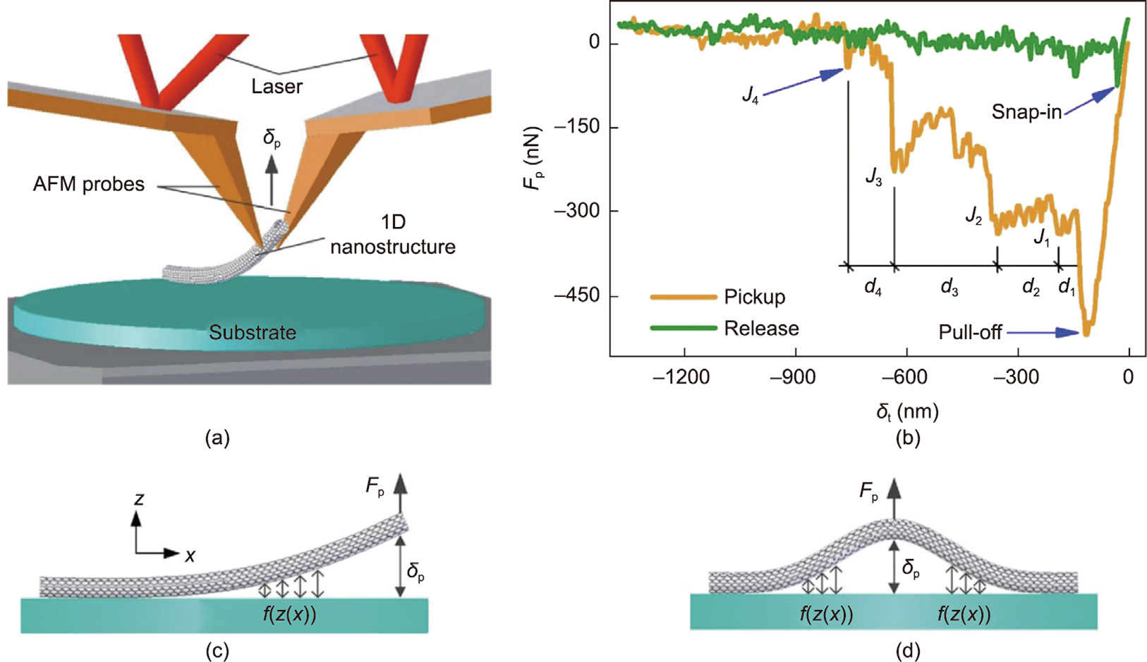
Fig. 8. Dual-microcantilever nanotweezers utilized by Xie and Régnier [110] (MS #11) for NW peeling. (a) Schematic of nanotweezer setup. Coordinated movement of the tips is used to peel Si NWs from a substrate by grasping at the end or center of an NW. (b) Force–distance approach and retraction curves for peeling an NW from its end. Discontinuous jumps are labelled J1–J4, with corresponding displacements labelled d1–d4. (c) Grasping and lifting an NW’s end induces peeling via a single crack front; (d) grasping and lifting via the NW’s center induces peeling via two crack fronts. δp: distance between peeling location on the NW and the substrate; FP: peeling force applied by microcantilevers; δt: nanotweezer displacement;  : NW–substrate interaction force per unit length. Reproduced from Ref. [110] with permission.
The experimental approaches presented by Strus et al. [77] (MS #7), Bhushan et al. [108] (MS #6), and Xie and Régnier [110] (MS #11) all depended on AFM microcantilevers to provide force– distance measurements during the adhesion and detachment of their 1D material from a substrate; the researchers subsequently computed the area bound by the force–distance curve to evaluate the total adhesion energy. It is important to consider that this novel approach to adhesion energy quantification comes with limitations and uncertainties. To be specific, regardless of the configuration of 1D material-microcantilever probe, the microcantilever component (whether it has a tip or is tipless) must be brought into close proximity to the substrate in order for the 1D material to effectively conform and form a line contact with the substrate. Consequently, the final approach segment and the initial retraction segment of the force–distance curve in all three studies corresponded to snap-in and snap-out of their respective microcantilevers, as shown in Figs. 6(c) and 7(d). Strus et al. (MS #8) distinguished which portion of the force–distance curve corresponded to the microcantilever snap-in and snap-out. This allowed the work associated with the microcantilever’s interaction with the substrate to be omitted. However, the physical connection between the 1D material and the microcantilever dictates that a significant segment of the 1D material will conform or be peeled off in order to facilitate the snap-in and snap-out of the microcantilever, respectively. Therefore, microcantilever snap-out will always obscure a portion of the 1D material’s peeling sequence on the force–distance curve. AFM facilities typically do not provide a means of monitoring the crack front during a 1D material’s peeling sequence. Therefore, a computed total adhesion energy value will, in any case, correspond to only an arbitrary length of the 1D interface. Hence, an adhesion energy per unit of adhered area or length cannot be accurately determined.
The AFM-based detachment techniques described thus far offer a clear advantage over static techniques in that they allow the interfacial condition over a significant length of a 1D interface to be examined through the evaluation of a force–distance curve. Nevertheless, clear uncertainties persist, as such techniques lack the capability to directly observe the deformed shape and adhered length of a 1D material during attachment and detachment. Direct observation of the peel front holds promise for facilitating the computation of an interfacial adhesion energy per unit length value, and could also help to clarify the relationship between the peeling force and the peel angle. Direct observation of a 1D material’s deflection shape also promises to elucidate whether shear forces and/or friction play an important role during detachment. In the next section, we explore detachment techniques that are capable of directly visualizing the deformation behavior of a 1D material of interest.
《4.2. Force–distance measurement with qualitative deformation visualization》
4.2. Force–distance measurement with qualitative deformation visualization
In 2009, Manoharan and Haque [111] (MS #12) used OM to directly observe the deformation behavior of an NW as it was brought in and out of contact with a substrate—a significant step forward in directly observing a 1D adhesion process. Here, the NW sample selected for study was large enough (Φ = 100 nm) to reflect sufficient light for the detection of its deflected shape using 100× microscope optics. The NW cantilevered out from a microelectro-mechanical system (MEMS) force sensor (fastened via EBiD) attached to a piezo-actuator, as shown in Fig. 9(a) [111]. The NW was positioned at the edge of a Si substrate under the optics, as shown in Fig. 9(b) [111]. The OM visualization permitted the microcantilever to be positioned at a small separation distance from the substrate edge, avoiding the issues associated with microcantilever snap-in described by Strus et al. [77] (MS #7). Under this configuration, the deflection of the NW as it adhered to the substrate during approach and retraction was normal to the focal plane of the optics, resulting in defocusing of the NW. During snap-in, only the NW tip became defocused, corresponding to an arc-shape single-point contact. During retraction, defocusing progressively receded along the NW’s length, corresponding to Sshaped peeling. Snap-out was observed as an instantaneous refocusing of the NW, at which point an adhesive force of 165 nN (Table 1) was obtained using the snap-out distance and the precalibrated stiffness of the sensor. Manoharan and Haque’s use of OM for pinpointing the instance of snap-out of an NW was novel [111]; yet, the observations were qualitative and therefore did not fully demonstrate the quantitative potential of OM.
The limited spatial resolution of OM limits its capacity to detect NWs with smaller diameters, as was noted by Mead et al. [76] (MS #4). In order to directly observe the deformation of smaller diameter NTs and NWs during interface formation and detachment, the higher resolving power of SEM is needed. Initially, SEM was used only for qualitative means: to aid in aligning the 1D material within the imaging plane and to validate the theorized deformation modes. In 2008 and 2009, Ishikawa et al. [112,142] (MS #13 and MS #14) conducted peeling of MWCNTs from HOPG, mica, and NaCl substrates within an SEM where the deformed state of the CNT could be directly observed. An MWCNT was attached to a pre-calibrated piezo-resistive self-sensing microcantilever, with the CNT oriented parallel to the substrate. SEM micrographs were obtained simultaneously with the recording of force–distance approach–retraction curves. This permitted the researchers to directly observe S-shaped peeling and arc-shaped deflection of the CNT, as per Fig. 9(c) [142]. The transition between deformation modes was also associated with a clear force discontinuity as shown in Fig. 9(d) [142]. In Ref. [112], a total adhesion energy value of 78 keV was obtained for an MWCNT by considering the entire area bound by the approach–retraction curves (Table 1). SEM observations in Ref. [142] directly showed that the end contact of a CNT tended to slide along the substrate during arc-shape deflection, confirming the assumption made by Bhushan et al. [105] (MS #6). The peeling force curves exhibited small regular perturbation and were associated with nanoscale intermittent adhesion resulting from atomic-scale stochastic sliding. Furthermore, longer CNTs tended to exhibit a number of relatively large discontinuities during peeling (Fig. 9(d)) and were associated with mesoscale intermittent adhesion resulting from poor conformation of the CNT on the substrate. Finally, higher peeling velocities were found to slightly decrease the peeling force during the transition to point contact, while increasing the pull-off force obtained during complete detachment.
《Fig. 9》

Fig. 9. (a, b) NW adhesion investigation using MEMS force sensor under an OM by Manoharan and Haque [111] (MS #12). (a) Schematic showing a ZnO NW cantilevered out from an MEMS force sensor as it is brought into contact with a Si substrate. (b) Optical micrograph of a cantilevered ZnO NW positioned above a Si substrate. The edge of the wafer is clearly visible, providing the ability to control the adhered length of the NW. (c, d) In situ SEM interfacial adhesion characterization between an SWCNT and planar substrate by Ishikawa et al. [142] (MS #14). (c) SEM micrographs showing various stages of peeling a CNT from a substrate. S-shape peeling occurs between frames C and D, and point contact occurs between frames E and F. (d) Force–piezo-displacement approach–retraction curve for a ‘‘long” MWCNT. The instances corresponding to the SEM micrographs are demarcated. Discontinuities associated with mesoscale intermittent peeling are demarcated. Fz: vertical force. (a, b) Reproduced from Ref. [111] with permission, (c, d) reproduced from Ref. [142] with permission.
The high resolution imaging capabilities of the SEM as demonstrated by Ishikawa et al. [112,142] not only successfully verified that a CNT transitions between deformation modes but also confirmed that sliding and friction play a major role in the detachment of 1D interfaces. Evaluating the adhesion energy through assuming equivalence to the total work done by the retracting microcantilever may therefore tend to provide an overestimation if the energy dissipating due to sliding is not accounted for. In addition to these discoveries, the SEM micrographs exposed the challenges of precisely aligning the probe and substrate within the focal plane of the SEM. More specifically, non-ideal alignment resulted in the formed interface being obscured behind the misaligned substrate (Fig. 9(c)). In that case, the position of the crack front during CNT peeling could not be determined, preventing determination of the CNT’s total adhered length. Yet, an accurate measure of the adhered length would be necessary for calculating an adhesion energy per unit contact length parameter. The obscured interface also prevented the described mesoscale intermittent adhesion exhibited by longer CNTs from being verified.
《4.3. Quantitative deformation visualization》
4.3. Quantitative deformation visualization
In 2007, Desai and Haque [113] (MS #15) were the first to use SEM to obtain visualizations of a 1D material in which the material’s deformed shape during attachment and detachment could be directly quantified. A ZnO NW was cantilevered out from the edge of a TEM grid [143] and mounted within the SEM chamber. The flat surface of a tipless microcantilever was brought into contact with the free end of the NW so that point contact occurred, as shown in Fig. 10(a) [113]. The NW’s deflection profile immediately before snap-out was clearly observable from the SEM micrographs. An Euler–Bernoulli beam theory model was used to approximate the deflection (Table 2); the corresponding computed adhesion force is provided in Table 1. This detachment-based approach was the first to quantify adhesion forces by using only the observed deflection profile of the 1D material, as opposed to relying on microcantilever force feedback or actuator displacement.
《Fig. 10》
Fig. 10. (a) In situ SEM observations by Desai and Haque [113] (MS #15). The SEM micrograph shows the snap-in of a ZnO NW onto the surface of a microcantilever. (b–d) In situ SEM interfacial adhesion characterization of a CNT fiber ring on planar Au film substrate by Zheng and Ke [114] (MS #16). (b) SEM micrograph of CNT ring as it is moved toward the substrate using the W NM tip. (c) Nonlinear elastica model, where the force applied by the NM tip is balanced by the adhesive forces at the contacting segment of the ring. (d) Theoretical ring deformation profiles approximated by the elastica model, where both a line contact and a point contact is simultaneously stable during retraction. (e–g) In situ SEM interfacial adhesion characterization of SWCNTs within a CNT fiber by Ke et al. [115] (MS #17). (e) SEM micrograph of CNT fiber suspended across a TEM grid window, with the inset showing a partially delaminated bundle with a dangling end. (f) Deformed shape of bundle within the vicinity of the peeling crack front. The coordinates are extracted from the SEM micrograph, and the curves are approximated via a nonlinear elastica model. (g) High resolution TEM micrograph of a typical bundled CNT fiber. (h–j) In situ SEM adhesion investigation of a CNT fiber on a planar Au film surface of a microcantilever by Chen et al. [125] (MS #18). (h) Schematic of the experimental setup inside the SEM. (i) Arc-shape deflection of a fiber with its end point in contact with an Au surface—referred to as the ‘‘positive” detachment configuration. (j) S-shape deflection with sliding of the 1D interface—referred to as the ‘‘negative” detachment. P: applied force; 2a: length of contact between the CNT ring and the substrate;  : per-unit-length vdW force;
  : distance from the location of adhesive contact along the x- and y-axis, respectively; s: arc length along the longitudinal axis of the CNT bundle; θ: angle between CNT longitudinal axis and the x-axis; A–F: points on the CNT bundle are demarcated; h: total deflection of the CNT bundle;
  : horizontal span of the CNT bundle; R, P, and M: the vertical reaction force, horizontal reaction force, and bending moment acting at point B—the point of adhesive contact between CNT bundle and substrate. (a) Reproduced from Ref. [113] with permission; (b–d) reproduced from Ref. [114] with permission; (e–g) reproduced from Ref. [115] with permission; (h–j) reproduced from Ref. [125] with permission.
Two breakthrough experiments by Zheng and Ke [114] (MS #16) and Ke et al. [115] (MS #17), both in 2010, were the first to achieve quantifiable visualization of 1D materials during peeling inside an SEM. In these works, SEM micrographs were obtained over the entire duration of the peeling process. The researchers then quantified the adhesion energies by evaluating the observed deformation behavior, rather than by relying on a dedicated force sensor or displacement feedback from an actuator. In both studies, the samples of interest consisted of CNT bundles. Such CNT bundles are similar to those investigated by Ke et al. [75] (MS #2). Conveniently, when the bundles were brought into contact with a W probe, they remained strongly adhered; therefore, no further fastening using EBiD or Joule heating was required.
In the work by Zheng and Ke [114], a CNT fiber was folded into a ring configuration by the precise actuation of a W probe so that it was aligned within the focal plane of the SEM. The ring was then repeatedly brought in and out of contact with an Au film/Si substrate. SEM observations during approach and retraction revealed that the ring formed a line contact on the substrate with two crack fronts, as shown in Fig. 10(b) [114], similar to the configuration that would later be implemented by Li et al. [109] in 2015 (MS #10). An elastica model was used to approximate the deflection shape of the ring, where the point load applied by the probe was balanced by the interfacial adhesive forces of the contacting ring segment, as shown in Fig. 10(c) [114] (Table 2). The deformation model was in good agreement with the experimentally observed ring profile during the entire attachment and detachment process.
Zheng and Ke [114] deduced from their theoretical model that two simultaneous deformation states were stable during the retraction process, which can be considered to be analogous to the bistable S-shape and arc-shaped deflection profiles exhibited by cantilevered CNTs as modeled by Strus et al. [77] (MS #8) and observed by Ishikawa et al. [142] (MS #14). More specifically, at a given pulling force, the ring could form either a line contact or a point contact with the substrate; the associated ring profiles are shown in Fig. 10(d) [114]. Despite this, the point-contact deformation profile was not observed experimentally. When the CNT fiber was brought into contact, the formed interface could not be observed, as it was obscured by the substrate itself. This resulted from the defocusing of a portion of the vertically aligned substrate, as it lay above the focal plane of the EB. This observation demonstrates how phenomena associated with the depth-of-focus in microscopy can introduce challenges regarding visualization, especially when the experimental configuration requires multiple components oriented in different spatial planes.
Ke et al. [115] (MS #17) induced a CNT fiber to peel from a suspended CNT bundle in order to characterize the adhesive interaction between the SWCNTs contained within the bundle. This work differs from most detachment-based studies discussed thus far, which have investigated the interfaces formed between a 1D material and a planar substrate. A suspended CNT bundle with partially delaminated fibers was obtained using the approach described in Ke et al. [75] (MS #2). The inset SEM micrograph in Fig. 10(e) [115] shows a partially delaminated fiber with a dangling end. The dangling end was adhered to an actuated W tip and subsequently pulled in order to further delaminate it from the main suspended fiber. Once the peeled segment was sufficiently long, and with the position and actuation direction of the W tip carefully controlled, steady-state peeling occurred at a relatively constant peel angle. Under this configuration, the elastic deformation of the CNT bundle was confined to within the vicinity of the peel front. The deflection shape during the peeling process was extracted from the SEM micrographs and fitted using the elastica model from Mikata [124] (Table 2). The extracted coordinates and elastica model fit at different stages of peeling—that is, at different crack-front positions—are shown in Fig. 10(f) [115]. The peeling force, defined by the elastica fit, provided the delaminated moment. The adhesion energy was then derived from the bending moment, as per the work of Goussev et al. [119]. This derivation is also considered valid for when large scale deformation occurs [144]. This derivation was also found to match that presented by Kendall [83] and was also utilized in the static approach by Ke et al. [75] (MS #2). The peel force and adhesion energy were found to be linearly proportional for a given peel angle.
In the work of both Zheng and Ke [114] (MS #16) and Ke et al. [115] (MS #17), the fibers were assumed to have a regular hexagonal arrangement of SWCNTs with approximate diameters of 1.36 nm. A high resolution TEM micrograph of a typical CNT bundle is shown in Fig. 10(g) [115]. In both studies, the interaction between the CNTs within a fiber and the interaction between the CNTs and the Au film substrate were considered to only occur via vdW interactions. Therefore, the adhesion energy could be determined from a known applied force by approximating the interaction via the LJ potential [85,86]. In this way, Zheng and Ke [114] determined an adhesion energy per unit contact length of 0.288 nJ·m–1 for the interface between an SWCNT and the Au film (Table 1). Similarly, Ke et al. [115] determined an adhesion energy per unit contact length between two SWCNTs ranging from 0.126 to 0.162 nJ·m–1 (Table 1). This value aligned well with the theoretically derived adhesion energy of 0.151 nJ·m–1 .
In 2016, Chen et al. [125] (MS #18) used both quantitative visualization and force sensing to assess the adhesion of peeling CNT bundles. By implementing both quantification methodologies simultaneously and comparing their discrepancies, the researchers were able to investigate how structural defects play a definitive role in the adhesive behavior of CNT bundles. A microcantilever was utilized as both the planar surface for interfacial contact with the CNT bundle and as the force sensor, similar to the work by Desai and Haque [113] (MS #15). A CNT bundle was cantilevered out from a W tip using EBiD for fastening and was actuated to come in and out of contact with the back surface of the microcantilever, as shown in Fig. 10(h) [125]. Both ‘‘negative” and ‘‘positive” detachment configurations were investigated, as shown in Figs. 10(i) and (j). Under each configuration, Elastica theory was used to approximate the experimentally observed deflection profiles and the vertical peeling force (Table 2). The modeled peeling force was then compared with the force detected by the microcantilever. Significant discrepancies between the experimental and modeled deflection profiles and the peeling force were observed when a defect was identified within the suspended segment of the CNT bundle. The presence of a defect on a CNT bundle was therefore shown to significantly alter both the bundle’s deflected shape and the associated peeling force.
In 2014, Roenbeck et al. [116] (MS #19) were able to visualize the deformed shape of large-diameter MWCNTs during peeling from graphene-on-copper foil and graphite substrates, as shown in Figs. 11(a) and (b). MWCNTs were adhered to a microcantilever and peeled at a constant peel angle from the substrate of interest under a configuration similar to that used by Ke et al. [115] (MS #17). The peeling force was determined from SEM observation of the microcantilever deflection and was used to derive the adhesion energy via a Kendall peeling analysis [79]. A finite element analysis (FEA) model was used to fit the experimentally observed CNT deflection shape in order to validate the Kendall analysis. The researchers recognized that the width of the 1D interface formed between a conforming MWCNT and a planar substrate was dependent on whether the conformed segment of the CNT under testing would flatten or collapse entirely under adhesive interactions. MD simulations were therefore used to determine the interfacial contact width associated with a given CNT diameter and shell number. The surface energies of MWCNTs corresponding to both a flattened and collapsed state are provided in Table 1.
《Fig. 11》
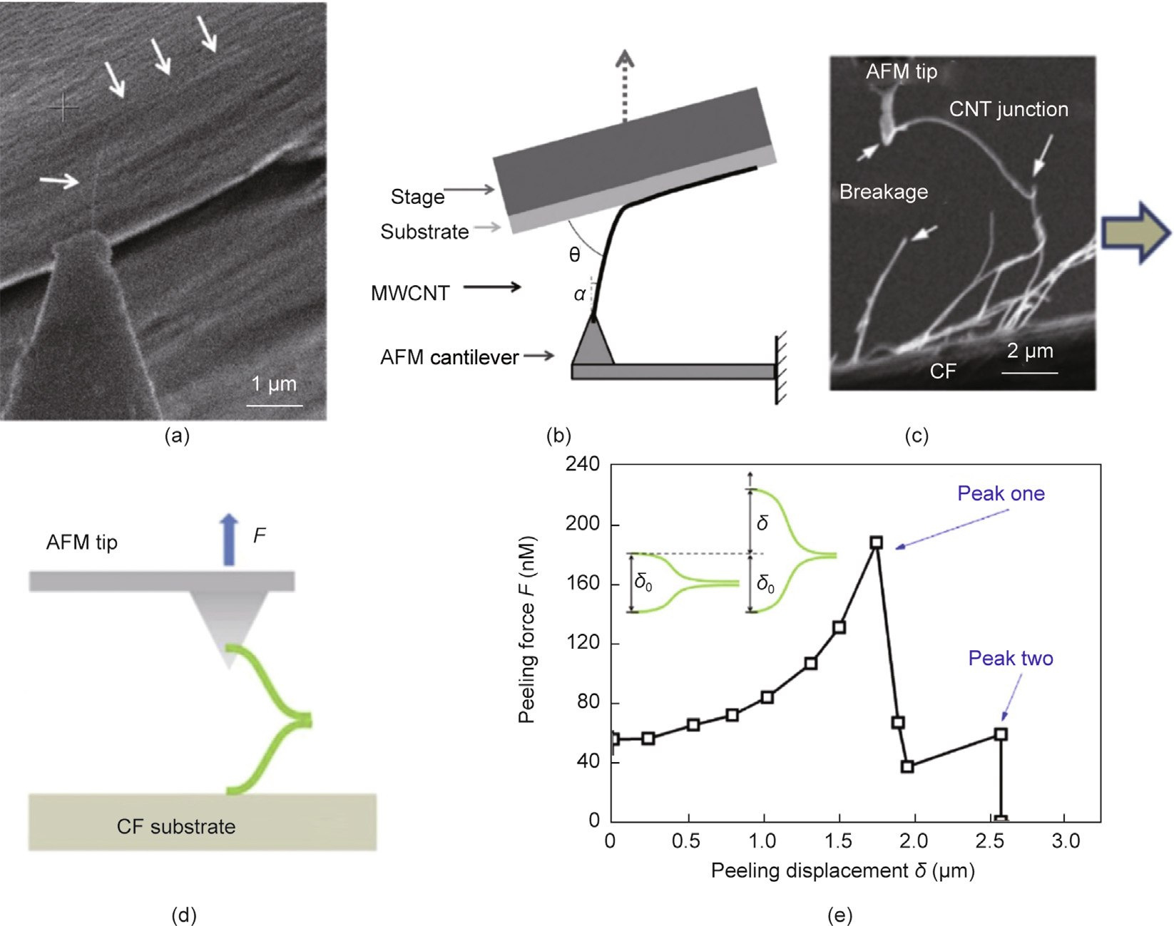
Fig. 11. (a, b) In situ SEM CNT peeling from graphene by Roenbeck et al. [116] (MS #19). (a) SEM micrograph; (b) diagram showing the peeling configuration of an MWCNT adhered to a graphene surface at an angle θ and with an offset α. (c–e) In situ SEM peeling of a CNT junction by Sui et al. [145] (MS #20). (c) SEM micrograph; (d) diagram showing peeling configuration; (e) peeling force–displacement curve. (a, b) Reproduced from Ref. [116] with permission, (c–e) reproduced from Ref. [145] with permission.
In 2016, Sui et al. [145] (MS #20) carried out in situ SEM separation of a sidewall-to-sidewall CNT junction. Such sidewall– sidewall junctions are one of a variety of CNT junctions that can be formed during the synthesis of continuous/macroscale CNT structures, including bundled CNT fibers and CNT networks/webs [146]. The structural integrity of these structures is dependent on the interfacial strength of the junctions rather than on the cohesive strength of a single CNT [147]. In the study by Sui et al. [145], CNT junctions tended to form during the CVD growth of CNTs on a CF. After locating a CNT junction, the dangling end of one of the CNTs was fastened to a self-sensing microcantilever using an EB curable glue, as shown in Figs. 11(c) and (d) [145]. During separation of the junction, the peeling force and SEM micrographs of the junction deformation were obtained simultaneously. The obtained force– displacement curve, shown in Fig. 11(e) [145], was distinct from those previously obtained for CNT–substrate peeling configurations. The CNTs of the junction tended to form symmetric Sshaped curves during peeling, followed by a spontaneous transition to arc-shapes—analogous to the transition exhibited by cantilevered CNT when peeled from a substrate. Each deformation mode was associated with a separate peak in the load–displacement curve.
The CNT bundles and large-diameter MWCNTs investigated in the last five previously discussed studies have large enough cross-sectional dimensions to be suitable for clear visualization using SEM. For example, the CNT bundles studied by Chen et al. [125] (MS #18) had a transverse width of 45 nm, and the MWCNTs studied by Roenbeck et al. [116] (MS #19) and Sui et al. [145] (MS #20) had minimum outer diameters of 19 and 80 nm, respectively. SWCNTs, on the other hand, have diameters as small as 0.34 nm (as characterized by Li et al. [109] (MS #10)). This is below the resolution limit of SEM and is therefore too small to obtain a quantifiable deformation profile. Thus, the SEM-based quantitative visualization approaches described here are not viable alternatives to the AFM-based force-sensing approaches presented, for example, by Buchoux et al. [108] (MS #9) and Li et al. [109] (MS #10).
In 2018, Mead et al. [15] (MS #21) were the first to use SEM to visualize NW peeling for adhesion energy assessment. ZnO NWs were cantilevered out from a Si substrate using OM-assisted NM in an ambient environment—the same manipulation strategy used by Mead et al. [76] (MS #4). The Si substrate was aligned vertically within the SEM, and the NW of interest was fastened to a W probe using EBiD Pt, as shown in Fig. 12(a) [15]. The W NM probe was then actuated to peel the NW from the substrate, where it formed an S-shaped deflection profile, as shown in Fig. 12(b) [15]. An Euler–Bernoulli beam model approximated the SEM-observed S-shaped deflection profile by assuming pure bending loading conditions (Table 2). The hexagonal cross-section of an NW was measured using high resolution SEM and was used to determine the width of the 1D interfacial area, where one hexagonal facet was assumed to conform to the substrate. The strain energy stored in the deflected segment of the NW was computed. By recognizing that a strain–adhesion energy equilibrium existed during the peeling, the researchers were able to determine the interfacial adhesion energy from the strain energy release rate. A nominal adhesion energy per unit contact area of (1.37 ± 0.28) J·m–2 was obtained for the interface formed by a ZnO NW on a Si substrate (Table 1).
《Fig. 12》
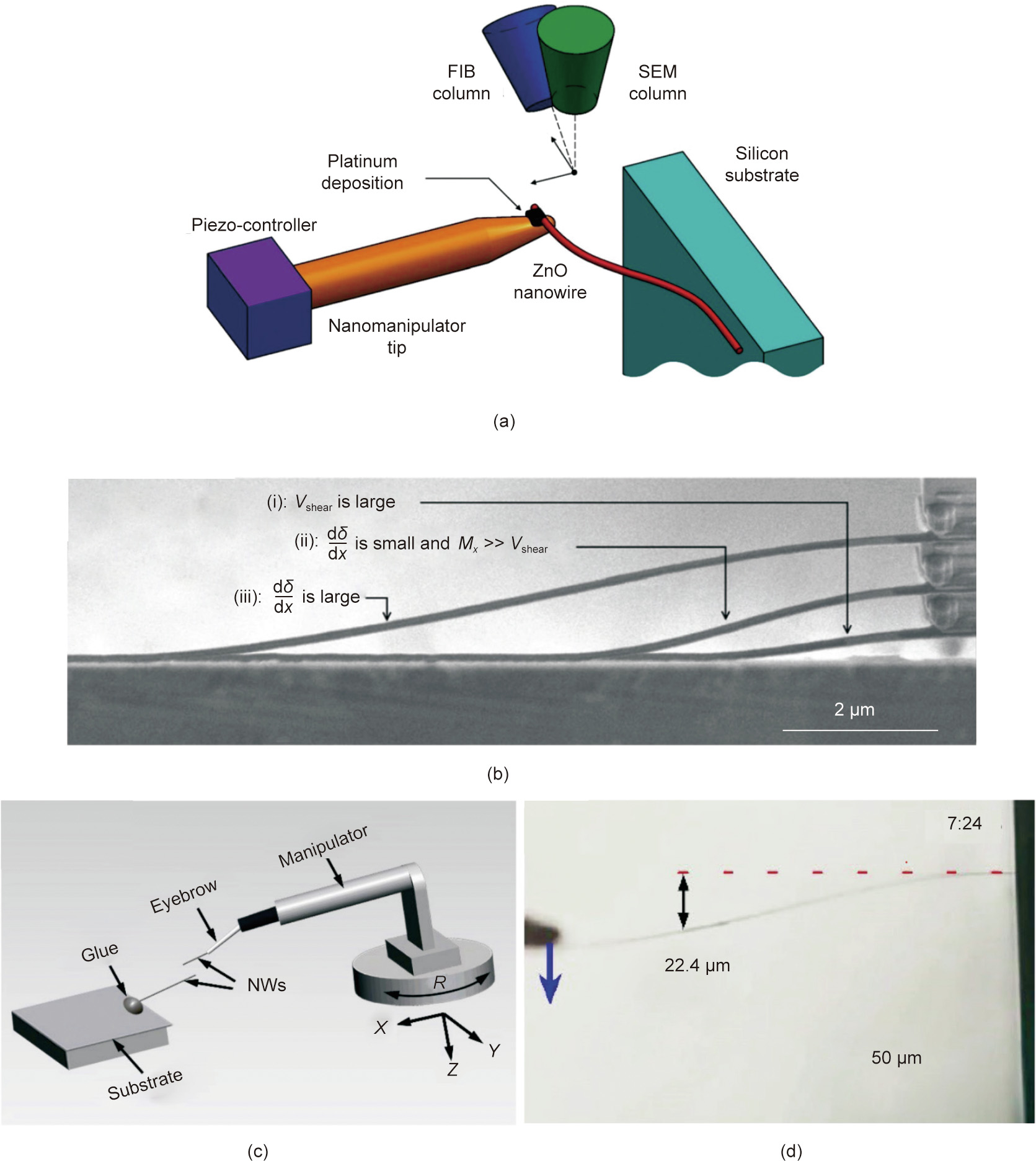
Fig. 12. (a, b) In situ SEM peeling of NWs from a planar substrate by Mead et al. [15] (MS #21). (a) Diagram of the NW peeling setup inside an SEM. (b) SEM micrograph showing the deflection shape of NW during peeling; at short detachment lengths (regime I) shear forces dominate, and at large detachment lengths (regime III) the slope of deflection becomes large. Vshear, Mx: shear forces, and bending moment experienced by the NW; δ: deflection of NW; x: distance from adhered end along the x-axis. (c, d) OMbased NW contact pair adhesion study by Cui et al. [122] (MS #22). (c) Diagram of NW contact pair configuration under OM. (d) OM micrograph of NW pair after establishing conformal contact. R: axis of rotation. (a, b) Reproduced from Ref. [15] with permission, (c, d) reproduced from Ref. [122] with permission.
Unlike the nonlinear elastica models [124] utilized by Zheng and Ke [114](MS #16), Ke et al.[115](MS #17), and Chen et al.[125](MS #18) to approximate the highly deformed profiles of CNT fibers, Mead et al.[15] utilized a much simpler linear Euler–Bernoulli beam model to assess the deformation of the relatively less compliant NWs. Mead et al. [15] recognized that the small-angle approximation [120] utilized by the linear model limited that model to assessing profiles with relatively small deflections. During the initial stages of peeling (regime I), when the detached length of the NW was small, the NW’s deflection profile was governed by shear forces and hence was Z-shaped (Fig. 12(b-i)). During the later stages of peeling (regime III), when the NW’s detached length was large, the corresponding slope of the NW’s deflection profile was also large (Fig. 12(b-iii)). Hence, the linear model was only valid for assessing part of an NW’s peeling regime (regime II).
In 2022, Cui et al. [122] (MS #22) demonstrated that OM was capable of quantitatively observing the deflected shape of NWs during peeling. The experimental setup is shown in Fig. 12(c) [122]. The attractive force between two cantilevered SiC NWs was quantified by bringing the NWs in and out of conformal contact, as shown in Fig. 12(d) [122]. Here, the deflection distance of one cantilevered NW was used to quantify the attractive force before snap-in, using an Euler–Bernoulli beam model that approximated the NW as a point-loaded cantilever (Table 2). By assessing the NW’s total deflection prior to snap-in, the researchers were able to provide a measure of long-range attractive forces, which were attributed to electrostatic interactions.
《5. Conformation of 1D materials, multi-asperity contact, and stick–slip behavior》
5. Conformation of 1D materials, multi-asperity contact, and stick–slip behavior
The condition of a 1D interface is not necessarily uniform along its length. As briefly mentioned in Section 3, this fact was recognized by Mead et al. [76] (MS #4) when attempting to explain why such a large standard deviation was present in the nominal adhesion energy value obtained for ZnO NW–Si substrate interfaces. A number of detachment-based techniques discussed in Section 4—including those by Manoharan and Haque [111] (MS #12) and Ishikawa et al. [142] (MS #14)—also led the researchers to deduce that the condition of their interfaces of interest were not uniform and that detected artefacts directly resulted from this nonuniformity. The complex and nonuniform condition of 1D interfaces and its effect on their adhesion behavior are explored in this section.
The facetted surface of the ZnO NWs investigated in both the static and peeling techniques developed by Mead et al. [15,76] (MS #4 and MS #22, respectively) was considered to be near atomically smooth. These NWs formed interfaces with Si substrates, which were also considered to be atomically smooth. Nevertheless, AFM examination of an exposed interfacial surface by Mead et al. [15] (MS #22) established that sub-nanometer surface features were in fact present at an NW–substrate interface. The surface features were deduced to originate from defects and/or contaminants distributed along the 1D interface, and will be explored in more detail in Section 8. To obtain a 1D interface with a continuous condition, the NW is therefore required to perfectly conform to these features. However, as explored by Xie et al. [148], the capacity of an NW to conform to a surface consisting of sub-nanometer surface features is dependent on its bending stiffness. The ZnO NWs investigated by Mead et al. [15,76] (MS #4 and MS #22) had a relatively high bending stiffness and therefore could not fully conform to the sub-nanometer surface features. Instead, contact of an NW with the substrate was considered to occur in a discrete manner, with contact only occurring at the apexes of the highest asperities. Such a condition can be referred to as ‘‘multi-asperity contact.” These discrete contact points imposed atomic-scale separation between the NW and substrate, leading to a variation in the interfacial condition along the length of the NW. The real contact area that exists at the nanoscale is a recurring problem in nanoscience and is discussed more broadly by Jacobs and Martini [149].
The tendency for a 1D material to conform via multi-asperity contact has significant implications in regard to the capacity of static adhesion tests to quantify adhesion values with low standard deviation. Specifically, in a static adhesion test, the crack front remains stationary. The position of the crack front is determined by the strain–adhesion energy equilibrium and is influenced by the interfacial condition only within its immediate vicinity. Consequently, the crack front location should be highly sensitive to any variation in the condition along the interface. The distribution of asperities along a 1D interface may therefore dictate the position of the crack front and thus lead to significant variation in the computed interfacial adhesion energy. Furthermore, the faceted surfaces of ZnO NWs facilitate the formation of large interfacial contact areas, in comparison with NWs with circular crosssections. One can theorize that the larger interfacial area of a ZnO NW facilitates a larger number of surface asperities at the interface. Consequently, it is expected that discrete interfacial contact is more prevalent for faceted and larger diameter NWs with a higher bending stiffness. Dissimilarly, NTs are highly conformal, as they have a significantly lower bending stiffness compared with NWs, have circular cross-sections, and typically exhibit minimal defects. Therefore, NTs are expected to exhibit a more continuous interfacial condition.
During the detachment of the ZnO NWs by Mead et al. [15] (MS #21), SEM snapshots taken over the entire peel progression of an NW revealed that the crack front did not progress at a constant rate along its 1D interface. The deflection profiles exhibited by an NW at different stages of peeling were compared via four composite micrographs (Fig. 13(a) [15]). The crack front was found to ‘‘stick” at certain locations along the interface, even as more strain energy was introduced to the NW via further deflection (Fig. 13(a), between snapshots ① and ② (part i), and snapshots ③ and ④ (part iii)). The crack front would then suddenly ‘‘slip” to another stick location without requiring the addition of further strain energy (Fig. 13(a), between snapshots ② and ③ (part ii), and snapshots ④ and ⑤ (part iv)). This stick–slip phenomenon was also observed when computing the NW’s stored strain energy over the duration of peeling. The progression of strain energy stored in the NW during peeling was plotted with respect to a normalized detached length parameter (Fig. 13(b) [15]). This sawtooth pattern shows the repeated build up and release of strain energy, and can be considered analogous to those exhibited in the force–displacement curves obtained during the peeling of CNTs by Ishikawa et al. [142] (MS #14). Both Ishikawa et al. [142] and Mead et al. [15] recognized that the stick–slip behavior was associated with a nonuniform interfacial condition resulting from an NW not fully conforming to the planar substrate surface. Ishikawa et al. [142] referred to this phenomenon as ‘‘mesoscale intermittent peeling.” As mentioned earlier, the stick–slip behavior observed by Mead et al. [15] can be explained by considered that the NW conforms to the substrate via multi-asperity contact. Thus, the positions where the sticking of the crack front occurred can be expected to correspond to asperity locations. Mead et al.’s conclusion [15] is also supported by Manoharan and Haque [111] (MS #12), who considered that their interface of interest was associated with multi-asperity contact. The researchers further clarified that the conformation of an NW is dependent on a balance between the bending resistance of the NW and the interfacial adhesive forces.
《Fig. 13》
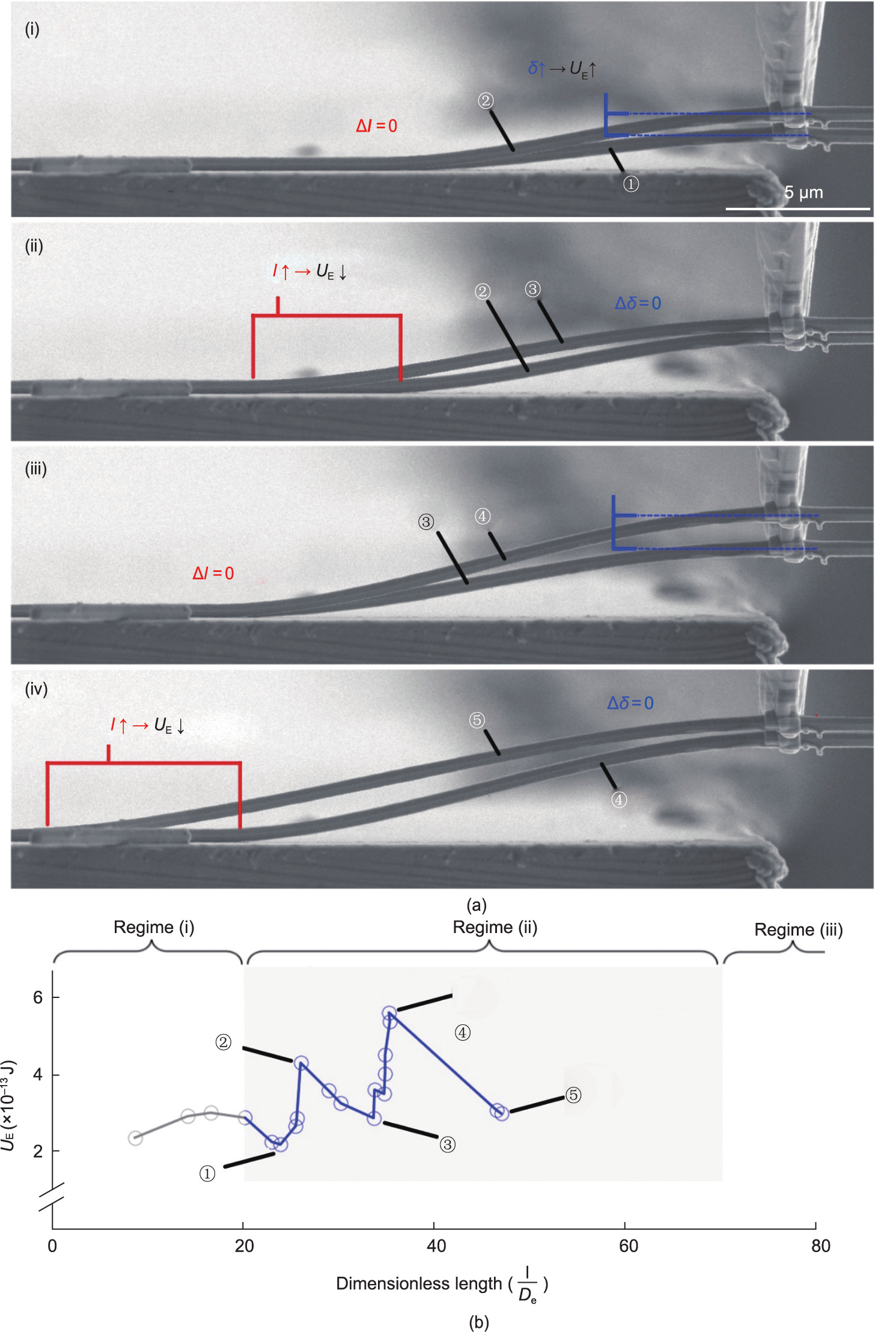
Fig. 13. (a) Composite SEM micrographs showing the S-shaped deflection profile of an NW as it is peeled from a substrate: (i) ‘‘Sticking” occurs as the crack front does not progress between snapshots ① and ②; (ii) ‘‘slipping” occurs as the crack front moves rapidly to the next sticking location between snapshots ② and ③; (iii) a second sticking event occurs between snapshots ③ and ④; and (iv) a second slipping event occurs between snapshots ④ and ⑤. (b) Strain energy progression plotted against a dimensionless detached length parameter; a clear sawtooth pattern can be observed, corresponding to the repeated buildup and release of strain energy. Labels ① to ⑤ demarcate which data points correspond to which snapshots. δ: deflection of NW;  : detached length of NW; UE: total elastic energy stored in NW; De: equivalent diameter of NW. Reproduced from Ref. [15] with permission.
The peeling study by Ke et al. [115] (MS #17), as well as all previously discussed static techniques [74–76,104] (MS #1, MS #2, MS #3, and MS #4), assumed that the position of the crack front was dictated by a strain–adhesion energy equilibrium, and that the strain energy release rate was therefore equivalent to the adhesion energy of the interface. During the peeling of CNT fibers by Ke et al. [115], the quantified strain energy release rate remained constant over the duration of the peeling. Maintaining this equilibrium was facilitated by the near-perfectly uniform interfacial condition that exists between single CNTs within a fiber. In contrast, Mead et al. [15] recognized that the condition of nonuniform multi-asperity contact prevented an equilibrium from being maintained. More specifically, the crack front initially sticks as the strain energy stored in the NW provides an insufficient driving force to overcome the resistance to delamination—the interfacial adhesion energy. The sticking is overcome when the strain energy exceeds the adhesion energy of the interface, permitting slipping to occur until another sticking site is reached. Therefore, a strain–adhesion energy equilibrium is not maintained over the duration of peeling; instead, it only exists at the instances when a sticking site is overcome. Consequently, Mead et al. [15] only evaluated the interfacial adhesion energy at local maxima in the strain energy release rate curve (the location of sticking sites). This recognition that a nonuniform interfacial condition will prevent a strain–adhesion energy equilibrium from being maintained draws attention once more to the limitations of techniques that apply quasi-static assumptions to evaluate an interface when the crack front remains in a single location.
The real contact area formed between a conforming NT and substrate is also complex. For example, Roenbeck et al. [116] (MS #19) clarified how strong interfacial adhesion between a CNT and substrate can cause significant radial deformation of the CNT. This radial deformation is dependent on the CNT’s diameter and shell number, and results in a dramatic increase in the CNT’s interfacial contact area. Fig. 4(e) diagrammatically illustrates the MD-simulated radial compression of CNTs with different diameters, induced by theoretical vdW interactions with a graphite substrate [87]. Due to this phenomenon, it is important to consider both the outer diameter and the shell number of a CNT when comparing its interfacial adhesion with energies obtained from CNTs in other studies.
《6. The coupling of adhesion and friction, and 1D arrays》
6. The coupling of adhesion and friction, and 1D arrays
《6.1. The coupling of adhesion and friction》
6.1. The coupling of adhesion and friction
To facilitate the straightforward evaluation of interfacial adhesion, the fundamental characterization techniques presented thus far typically seek to induce interfacial delamination under modeI loading conditions. More specifically, the 1D materials in these techniques are constrained in a manner that induces pure bending or buckling deformation, while avoiding significant shear deformation. In this way, delamination is considered to be induced via the application of normal forces at the interface. However, the vast majority of these experimental techniques are implementing by actuating a probe or microcantilever (on which the 1D material is fastened) to move in a single direction or along a single axis— often perpendicular to the substrate surface. Yet, under the specific context of an S-shape peeling configuration, actuation along two axes simultaneously (perpendicular and parallel to the substrate surface) is required to avoid applying an axial force to the 1D material. The SEM observations made by Mead et al. [15] (MS #21) provide an example of the shear-dominated deformation of a 1D material—in this case, during the initial stages of peeling (Fig. 12(b-i)). An interface that experiences both normal peeling forces (mode I) and shearing forces (mode II), in what is also defined as ‘‘mixed-mode” peeling, while exhibit different delamination behavior from an interface that experiences only normal forces [72]. In particular, the energy required to separate an interface is not the same under mode-I and mode-II delamination [150].
Techniques that rely entirely on the force feedback from a microcantilever [35,105,107,110] (i.e., MS #5, MS #6, MS #8, and MS #11) only detect normal forces; hence, shearing forces remain undetectable. For example, to initiate peeling, the approachretraction procedures conducted by Strus et al. [107] (MS #8), Bhushan et al. [105] (MS #6), Xie and Régnier [110] (MS #11), and Manoharan and Haque [111] (MS #12) actuated the microcantilever perpendicular to the substrate surface. The resulting geometric constraint on the 1D material can be expected to introduce shear forces. This constraint is particularly severe in experimental setups where the 1D material is rigidly fastened to the microcantilever [77,105,111] (MS #6, MS #8, and MS #12), as the end of the 1D material cannot realign in the direction of the force. Furthermore, pure-bending mechanical deformation models, such as that used by Mead et al. [15] (MS #21), provide an inaccurate evaluation of interfacial adhesion if shear forces are present.
If the shear forces applied to a 1D material are large enough to overcome the static friction associated with its contact interface with a substrate, sliding of the 1D material may occur. Sliding of the interface was observed during the ‘‘negative” deformation configuration investigated by Chen et al. [125] (MS #18) and was considered to be responsible for the sawtooth force–displacement behavior observed by Bhushan et al. [105] (MS #6). Interfacial sliding due to induced shear forces may also offer an alternative mechanism (aside from a nonuniform interfacial condition) that explains the presence of discontinuities observed in the force– distance curves obtained by Strus et al. [77] (MS #8), Xie and Régnier [110] (MS #11), and Ishikawa et al. [142] (MS #14).
The experimental observations described above demonstrate that the detachment of a conformed 1D material is typically associated with some degree of mixed-modality, whereby peeling (mode I) and shearing forces (mode II) act to delaminate the interface. In addition, the final stage of a detachment process is typically associated with the transition to an arc-shape deflection curve and single-point contact, where the point contact tends to slide along the substrate surface. In light of these experimental observations, the friction and adhesion behavior of a 1D material can be considered to be coupled. In fact, it may not be practically conceivable to experimentally observe these tribological characteristics in complete isolation. MD simulations have further established that the adhesion and friction behaviors of a 1D material are unavoidably coupled during detachment processes [91].
Experimental studies that evaluate the friction behavior of 1D materials are critical in understanding their detachment/peeling behavior and the coupling of adhesion and friction. The friction behavior of 1D materials has been extensively investigated, as inducing a 1D material to slide across a substrate is simpler to implement experimentally than detaching it from a substrate. Lateral force microscopy (LFM) using an AFM has been commonly applied to study the friction and rolling behavior of NWs on various substrates [151–155]. AFM-based LFM has also been used to study the adhesion of BNNTs on Si substrates [156]. The use of an NM to induce the sliding of NWs under OM-based observation has proven to be a successful approach for characterizing both the static and dynamic friction of NWs on substrates with varying composition, surface roughness, and textures [130,148,157–163]. SEM-based friction tests have also been developed [164–168]. Static and dynamic friction models were developed by Dorogin et al. [169,170] and applied to SEM and AFM data. A review on characterizing the friction of 1D materials has been provided by Guo et al. [171].
《6.2. 1D arrays for biomimetic adhesives》
6.2. 1D arrays for biomimetic adhesives
The applications of 1D materials drive which geometric configurations and interfacial components are selected for adhesion assessment in the literature. Most of the early characterization techniques—including the majority of those discussed thus far— sought to investigated the interface between a 1D material and a substrate, as it is separated under mode-I loading conditions. The objectives of these studies were set in response to the design and demonstration of a vast array of novel devices and probes with integrated 1D components, where the interaction between the 1D material and an adjacent surface was of primary concern. However, in recent years, there has been a shift in focus toward the integration of 1D materials into array architectures for biomimetic adhesives and as reinforcement agents in emerging nanocomposites. In such applications, shear forces (or mode-II loading) play a more significant role. For biomimetic adhesive applications, the behavior of the interfaces formed between adjacent 1D materials is of critical importance and will be discussed in this section. For nanocomposite applications, the interface formed between an embedded 1D material and its surrounding matrix, as well as the shear strength of the 1D material itself, becomes of primary relevance and will be explored in Section 7 [172].
By mimicking the complex hierarchical structures found on adhesive surfaces in nature, synthetic architectures based on 1D arrays provide unparalleled dry reversible adhesive performance. The adhesion behavior of biomimetic adhesives based on CNT arrays has been extensively investigated [45–57]. Here, the incredible adhesive behavior of a 1D array is tied to these materials’ ability to buckle and conform to a surface and has been theoretically evaluated using multiscale models incorporating both MD and FEA simulations [173]. The adhesive interaction between the adjacent parallel aligned 1D materials within the array itself also plays a critical role in the overall adhesive performance. The tendency for vertically aligned 1D materials to clump together was investigated by Zhou et al. [30]. Clumping between CNTs [174], as well as between NWs [175–179], has been observed and investigated. The clumping of 1D materials is illustrated in Figs. 14(a)–(c) [30,177]. The tendency of 1D materials to clump depends on their resistance to bending and separation distance, as well as their adhesive interaction. During clumping, 1D materials tend to make contact with each other at or near their free ends and may form a cross-contact, as shown in Fig. 14(a). Here, the transition from side–side and tip–side to tip–tip contact is analogous to the transition from line contact to point contact observed in 1D material– substrate configurations. SEM micrographs showing the clumping of vertically aligned ZnO within an array are provided in Figs. 14(b) and (c). As demonstrated by a number of experimental [145,180–182] and theoretical [183,184] CNT junction detachment studies, forces that induce the detachment of an interface may not necessarily remain aligned perpendicular to the interface. Hence, the transition between deformation configurations and the final detachment from point contact are dictated by lateral shearing rather than normal adhesive forces.
《Fig. 14》
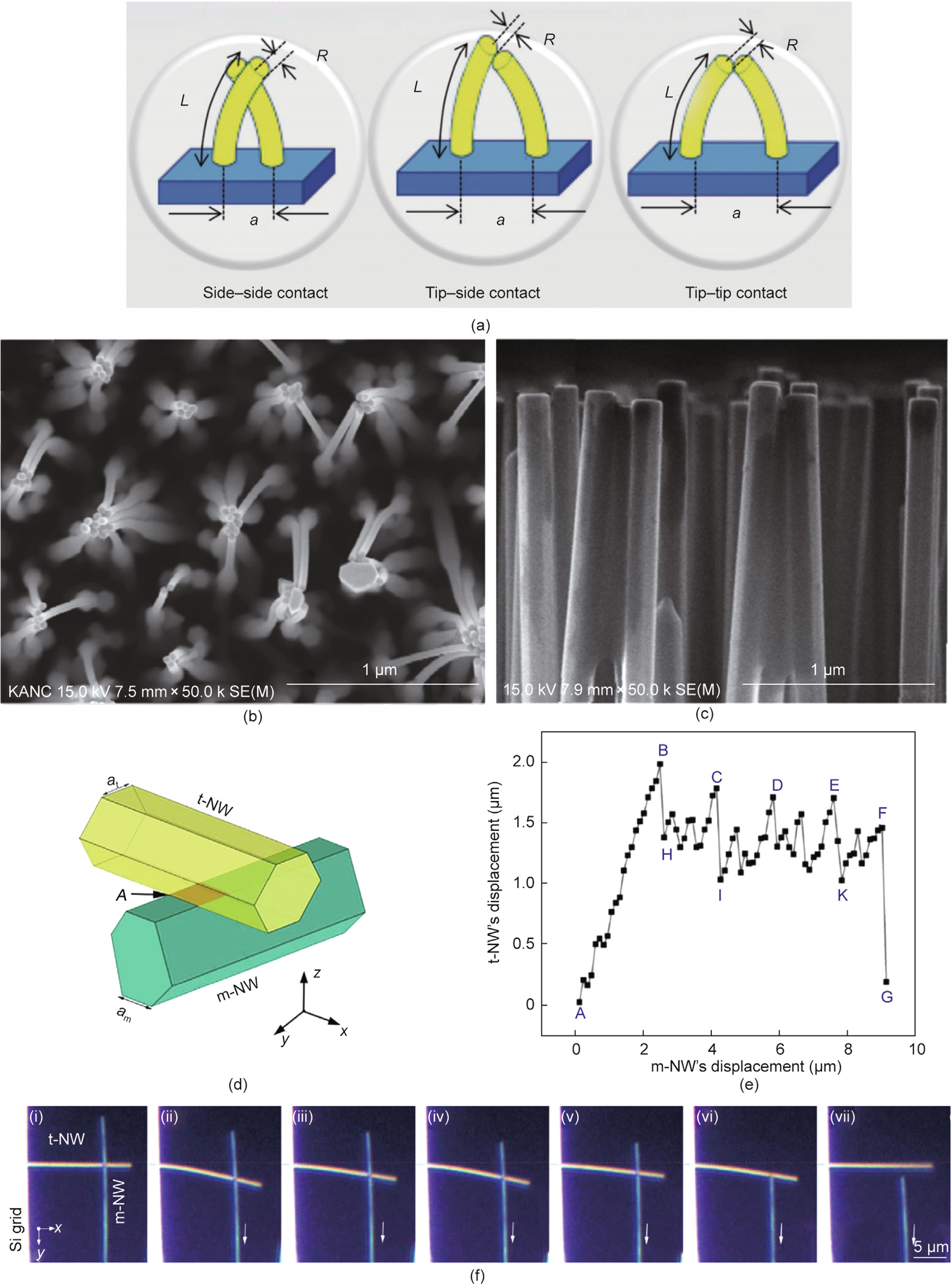
Fig. 14. (a) Schematic illustration showing the clumping of vertically aligned fibers, forming side–side, tip–side, and tip–tip contact. (b, c) SEM micrographs showing clumping in a ZnO NW array. (d–f) NW pair shearing investigation carried out by Yibibulla et al. [188]. (d) Schematic showing the configuration of an NW contact pair. The upper and lower NW are demarcated by t-NW and m-NW, respectively. (e) Deflection of the t-NW with respect to the displacement of the m-NW during shear progression. The deflection–displacement curve exhibits a sawtooth pattern corresponding to stick–slip behavior. Notable data-points are labelled A–G. (f) Series of OM snapshots showing the deflection and displacement of the NW contact pair during shear progression. Each snapshot, labelled (i)–(vii), correspond to the demarcated datapoint on the deflection–displacement curve in part (e). R: radius of fiber; L: length of fiber;  : spacing between fibers;
  : facet length of the t-NW and m-NW; A: location of contact between the two NWs. (a) Reproduced from Ref. [30] with permission, (b, c) reproduced from Ref. [177] with permission, (d–f) reproduced from Ref. [188] with permission.
Whether considering the conformation of a 1D array when pressed onto a substrate [185] or investigating the interaction between adjacent 1D materials within an array, it is apparent that adhesion and friction behavior are intertwined [44]. Experimental techniques that fundamentally investigate the attachment, detachment, and sliding interactions between pairs of 1D materials are thus particularly relevant to biomimetic adhesive application. In this context, Bhushan et al. [105,186] explored the sliding interaction between CNT pairs, and Xie et al. [187] and Yibibulla et al. [188] investigated the coupling of adhesion and friction between NW pairs. Yibibulla et al. [188] formed a suspended crossjunction between two perpendicularly aligned NWs, as shown diagrammatically in Fig. 14(d). The lower NW, referred to as ‘‘mNW,” was then induced to move along its longitudinal axis using an NM under OM observation. This movement caused the adhered or ‘‘stuck” upper NW, referred to as ‘‘t-NW,” to deflect in the direction of movement of the m-NW. When t-NW reached a critical deflected state, it began to slide or ‘‘slip” back to a less deformed state. The t-NW would then again ‘‘stick,” and the process repeated. This stick–slip behavior was observed as a sawtooth pattern in the obtained deflection–displacement curve, as shown in Fig. 14(e) [188]. A series of OM snapshots showing the interaction of the NW pairs is also provided in Fig. 14(f) [188].
《7. Embedded 1D materials in nanocomposite applications》
7. Embedded 1D materials in nanocomposite applications
The mechanical performance of a filler–matrix composite is dependent on the capacity of the interface between the filler and matrix to transfer loads. Regardless of whether the filler/reinforcement agent consists of conventional microscale CFs or emerging 1D materials such as CNTs, the interfacial load transfer remains a decisive characteristic. A review by Desai and Haque [67] in 2005 explored how the mechanical properties of the interface influence the overall mechanical performance of a CNT–polymer nanocomposite, as did a study by Chen et al. [189] in 2018. In order to develop novel composite materials with enhanced and tailored mechanical properties, experimental techniques capable of quantifying interfacial load transfer are essential. It is in this context that the difference between microscale fibers and 1D materials becomes apparent. To be specific, quantitatively characterizing the mechanical behavior of 1D interfaces within nanocomposites poses a significant experimental challenge due to the reduction in characteristic length [190]. The interfacial shear strength (IFSS) and interfacial fracture energy (IFE) are established quantitative properties used to assess the load-transfer capability of such interfaces when undergoing ductile or brittle failure, respectively [191,192]. A variety of nanomechanical characterization techniques have been developed for quantifying the shear stress and fracture energy of the 1D interfaces within nanocomposites. The availability of such quantitative methodologies has permitted researchers to enhance the mechanical performance of nanocomposites by controlling the size, geometry, and dispersion of the 1D filler, as well as through surface modification [189].
Barber et al. [193–195] carried out both ex situ and in situ SEM pull-out tests on individual CNTs to investigate the 1D interfaces within CNT–reinforced polymer–matrix nanocomposites. The general approach involved attaching a CNT to the end of an AFM microcantilever, then embedding the free end into a polymer melt with a known embedded length. Once the matrix had solidified, the AFM microcantilever was actuated to pull out the partially embedded CNT, where deflection of the microcantilever provided a measure of the pull-out force, Pc. Barber et al.’s first studies [193,195] carried out the pull-out test ex situ using a commercial AFM system to measure the microcantilever deflection. Later, the pull-out tests were carried out on CNTs with varying embedded lengths inside an SEM. SEM observation was used to measure the microcantilever deflection, but also to determine whether failure occurred via CNT pull-out or fracture [194]. The Pc was found to increase proportionally with the embedded length of the CNT whilst the embedded length remained relatively short, and the IFSS was computed using a shear lag-model [192]. Chen et al. [196– 198] also carried out in situ SEM pull-out tests to investigate polymer nanocomposites using BNNT and CNT reinforcement agents, and polymethyl methacrylate (PMMA) and epoxy matrices. Distinct from general methodology utilized by Barber et al. [193– 195], Chen et al. [196–198] relied on first producing a fracture surface in a hardened composite in order to expose partially embedded/exposed NTs for testing. The NTs were then fastened to an AFM microcantilever in preparation for pull-out. In Chen et al.’s 2015 study [197], the embedded length of the tested CNT was determined after pull-out by measuring the length of the exposed CNT segment using SEM. Chen et al. [198] observed that Pc for BNNTs tended to plateau above a critical embedded length, and deduced that brittle interfacial fracture occurred preferentially to shearing. The Pc within this plateau region was used to determine the IFE [191]. Later, in 2017, 2018, and 2019, Yi et al. [204–206] successfully used a similar preparation approach to produce thinfilm CNT–aluminum, CNT–titanium, and BNNT–silica matrix composite samples with exposed fracture surfaces containing partially embedded/exposed CNTs and BNNTs, respectively. The in situ SEM pull-out configuration used for the BNNT–silica composites is shown diagrammatically in Fig. 15(a) [206]. SEM micrographs of a BNNT before and after fastening to the AFM tip and after pullout are shown in Fig. 15(b) [206]. Individual CNT pull-out tests have also been carried out on CNT–aluminum matrix composites by Yamamoto et al. [199] and Zhou et al. [200]. Tsuda et al. [201] proposed an in situ SEM technique for pulling out a CNT embedded in PEEK, where the CNT’s embedded length was controlled by FIB milling through-thickness holes into the polymer matrix behind the exposed CNT. This novel approach eliminated the requirement to directly measure the embedded CNT length after pull-out. In 2011 and 2014, Ganesan et al. [202,203] used a nanoindenteractuated push–pull MEMS to carry out in situ SEM pull-out tests on individual CNTs embedded in epoxy. The force–distance curve generated by the nanoindenter was used to quantify the interfacial shear stress and fracture energy for CNTs with different surface treatments.
Cooper et al. [210] observed the bridging of CNTs across a cavity in a microtome-sliced thin-film epoxy nanocomposite sample under TEM. Each end of the CNT of interest was securely embedded into the epoxy matrix. The ‘‘bridged” CNT provided the unique opportunity to induce pull-out by applying a lateral force via dragging a scanning probe microscope tip over the sample surface. Nie et al. [207] formed similar bridged CNT samples with their ends embedded in a PMMA thin film, as shown by the SEM micrograph in Fig. 15(c). The pull-out of a CNT was then induced by applying a lateral force via an AFM tip without the need to fasten the CNT to the tip, as illustrated in Fig. 15(d) [207]. The thin PMMA film permitted Nie et al. [207] to directly observe the embedded length of the CNT using SEM (Fig. 15(d)). Direct observation of the embedded segment of the CNT allowed the researchers to confirm that no kinking or entanglement had occurred within the matrix. Reviews on experimental techniques for characterizing the interfaces of CNT–polymer nanocomposites, including quantifying interfacial shear stress, were published by Chen et al. [211] in 2019 and Mani and Sharma in 2022 [212].
In a number of CNT pull-out experiments in which CNT fracture was preferentially induced over pull-out, observed that CNT fracture could occur via a ‘‘sword-in-sheath” failure mode [199]. This phenomenon—also referred to as telescopic pull-out—involved the separation of the inner and outer shells of MWCNTs [197]. These observations demonstrated how the interaction between the inner and outer shells of MWCNTs can play a significant role in the mechanical performance of CNT-reinforced nanocomposites. Controlled sliding between the inner and outer shells of MWCNTs was induced via an in situ SEM pull-out test using a nanomanipulator, as presented by Zhang et al. [208,209]. The applied experiment pull-out configuration is presented in Fig. 15(e) [208]. Here, the centimeter-long segment of the inner shell could be continuously pulled from the outer shell with a tube-length independent friction force of 1 nN. The cross-section of an MWCNT as the inner tube slides past the outer tube is schematically illustrated in Fig. 15(f) [209]. This nanoscale phenomenon is referred to as superlubricity, and is being extensively investigated [213,214]. The topic of superlubricity in MWCNTs is also discussed in a review of low-dimensional friction by Guo et al. [171].
《Fig. 15》

Fig. 15. (a, b) In situ SEM pull-out test for pulling out a BNNT partially embedded in a silica matrix, implemented by Yi et al. [206]. (a) Experimental configuration. (b) SEM micrographs showing a partially free BNNT: (i) prior to being fastened to the AFM tip; (ii) after being fastened to the AFM tip; and (iii) after being pulled out from the silica matrix. The newly exposed segment of the BNNT can be measured. (c, d) ‘‘Bridged” CNT pull-out tested implemented by Nie et al. [207]. (c) SEM micrograph of CNT, with each end embedded into a PMMA matrix. Embedded segments can be observed. (d) 3D diagram of an AFM tip being brought into contact with the suspended segment of a CNT in preparation for pull-out via the application of lateral force. (e) Schematic of the pull-out test configuration used to induce sliding of the inner shell from the outer shell of an MWCNT. The cut location is indicated, and is used to dictate the pull-out length. (f) Schematic of the cross-section of an MWCNT, where the inner shell slides over the outer shell. Springs indicate vdW bonding. (a, b) Reproduced from Ref. [206] with permission, (c, d) reproduced from Ref. [207] with permission, (e) reproduced from Ref. [208] with permission, (f) reproduced from Ref. [209] with permission.
Polymer composites can also be reinforced by CNT networks [215] or CNT bundles [216,217], and CF composites can be reinforced by a CNT interphase [218]. In such composite architectures, the interfacial strength between entangled or partially adhered CNTs and the interfacial interactions between the CNTs within a bundle play a definitive role in the final mechanical performance of the composite. For CNT-bundle-reinforced composites, the studies by Zheng and Ke [114] (MS #16), Ke et al. [115] (MS #17), and Chen et al. [125] (MS #18) are particularly relevant, while the study by Sui et al. [145] (MS #20) is pertinent to CNT networks and interphases. Although the majority of pull-out tests to date have investigated embedded CNTs, an in situ SEM test was developed by Zheng et al. [219] for quantifying the interfacial shear stress between individual ZnO NWs grown on CF. In the studied system, ZnO NWs acted as an interphase and improved stress transfer in CF hybrid composites.
《8. Environmental conditions and their influence on interfacial interactions》
8. Environmental conditions and their influence on interfacial interactions
The primary purpose of characterizing 1D interfaces is to better inform the design of devices which integrate 1D materials. In order for the respective characterization technique to be useful, the 1D material under test must exhibit adhesive behavior that is analogous to that which would occur within a final device. Likewise, an adhesion energy values obtained during testing must be representative of that which would be exhibited within a final device. Within this context, the techniques presented by Mead et al. [15,76] in 2018 (MS #21) and in 2020 (MS #4) characterized ZnO NW–Si substrate interfaces using NWs from the same sample batch and with a comparable diameter range. The experimental approaches were distinct; peeling tests in the 2018 study were carried out inside an SEM environment, while static arch tests in the 2020 study were implemented in an ambient environment. However, the obtained interfacial adhesion energies showed an order of magnitude discrepancy: (1370 ± 280) mJ·m–2 inside the SEM, compared with (51 ± 32) mJ·m–2 in air. Such a discrepancy begs the question—which measured adhesion energy can be used to inform the design of a device in which the ZnO NWs are to be integrated? What is the origin of this discrepancy? This section explores the critical role of the sample preparation and characterization environment on the adhesive behavior exhibited by a 1D material during testing.
The environment in which an interface is formed dictates what atoms are physically present at the interface and therefore what interfacial interactions can occur. After the formation of a 1D interface, the interface still remains susceptible to modification by the surrounding environment simply due to its 1D nature. To be specific, the entirety of a 1D interfacial area lies in close proximity to the interface edge, and therefore remains exposed to the environment. The volume of the 1D material itself, with its small cross-sectional dimensions, also constitutes are poor physical barrier for shielding the interface from the environmental. This is in contrast to a macroscale interface, in which the majority of the interfacial area lies far from the interface edge, and is also shielded from the environment by the large macroscale volumes of the interface constituents. Consequently, the adhesive behavior of a 1D material— a behavior fundamentally governed by interfacial interactions—is particularly susceptible to alteration by its surrounding environment. In the context of characterization, the sample preparation environment (when the interface is formed) and the testing environment (prior and during detachment) critically influence the observed adhesive behavior and measured interfacial adhesion energy of the 1D material of interest. In the context of final applications, the environment in which a 1D material is integrated into a device, how the component is encapsulated, and the final operation environment of the device dictate the 1D material’s adhesion behavior. The ambient environment of cleanrooms are controlled to maintain a 30%–40% relative humidity and temperature below 21 °C [220]. Microelectronics utilized in the aerospace industry are expected to operate reliability within a temperature range of –55 to 225 °C [221].
Characterization techniques performed on 1D materials in an environment that is analogous to final device condition can be expected to provide the most representative interfacial adhesion energy values, and therefore should be preferred. Most devices that integrate 1D materials are fabricated in a cleanroom environment, and are subsequently hermetically sealed or operated in ambient conditions, and therefore characterization techniques performed in air environments are of particular relevance. Ideally, the characterization environment should be precisely controllable, while also permitting the methodical investigation of adhesion under different environmental conditions, including relative humidity and temperature. Such capabilities permit researchers to isolating how specific interfacial interaction influence adhesion and also to determining the range of environmental conditions over which a device can effectively operate.
Many of the quasi-static adhesion characterization techniques explored in Section 4 relied entirely on force–displacement measurements obtained from microcantilever probes that were installed within an AFM setup. In these experimental setups, OBD, interferometry, or piezo-resistive-based microcantilever readout strategies were utilized, permitting testing of the 1D material of interest to be conducted in an ambient environment. AFMbased techniques can also support testing under controlled environmental conditions by placing the AFM inside an environmental chamber. For example, Strus et al. [107] (MS #7) carried out CNT force spectroscopy tests inside an environmental chamber backfilled with dry nitrogen, reducing humidity. By reducing humidity, Strus et al. [107] aimed to determine how vdW interactions contributed towards the adhesion of the CNT in isolation from capillary forces. The versatility of the AFM in being able to operate in different environments is well suited for adhesion characterization, but the tool does not facilitate direct visualization of the 1D material under test. All quasi-static techniques discussed in this review that enable direct visualization do so using OM, SEM, or TEM. Like the AFM, OM is also typically carried out in an ambient environment, and can also be used in combination with an environmental chamber. Nevertheless, the use of OM to investigate 1D interfaces has been somewhat overlooked due to its limited spatial resolution capabilities. Researchers have instead preferred to rely on the high spatial resolution of SEM and TEM. However, these facilities require the 1D material of interest to be placed inside a vacuum environment to reduce scattering of the EB prior to sample interaction. Furthermore, electron microscopy (EM) subjects the sample to electron irradiation—SEM and TEM typically utilize EBs with acceleration voltages up to 30 keV and within the range of 80–200 keV, respectively. Once a 1D material is placed inside the evacuated and electron irradiated environment of an EM, its interface is susceptible to modification, and its adhesion behavior risks being altered. A number of in situ SEM techniques carry out both formation and detachment of the 1D interface of interest inside the microscope chamber; for example, Roenbeck et al. [116] (MS #19) and Zheng and Ke [114] (MS #16). In other techniques, the interface remains intact prior to the sample being loaded into the microscope chamber; for example, Sui et al. [145] (MS #20), Ke et al. [115] (MS #17), and Mead et al. [15] (MS #21).
In order to investigate how the SEM environment can modify an NW–substrate interface during peel tests, Mead et al. [15] used AFM to examine the topography of a portion of the surface of a Si wafer that was left exposed after the detachment of an NW. High resolution micrographs showing the topography of representative exposed interfacial regions are shown in the AFM micrographs in Figs. 16(a) and (b) [15], respectively. Figs. 16(a) and (b) [15] show interfacial regions where high resolution SEM examination had not, and had been conducted earlier, respectively. Cross-sections of the topography are also illustrated in Fig. 16(c) [15]. In Fig. 16(a), residue could be found at the horizontally orientated interface, forming two ridges, separated by a distance that matches the width of the facet of the previously adhered NW. The researchers considered that this residue originated from the sample preparation procedure conducted outside of the SEM. To be specific, the NW had been placed onto the substrate while within an ambient environment, so that the thin layer of water molecules present on each component’s surface had migrated to form a meniscus at the edge of the 1D interface. It is expected that within this meniscus were some contaminants originating from either or both the sample surface and/or the ambient atmosphere. Once the sample was placed in vacuum, the moisture was vaporized, leaving the layer of solid contaminants behind at the interface. The persistence of absorbed hydrocarbons and other ‘‘third bodies” at nanoscale interfaces in air, and the implications for adhesion and friction is discussed by He et al. [222] and Bhushan [223]. In Fig. 16(b), thin rectangular-shaped layers of residue can be seen along the interface, corresponding to the field of view of the SEM during high resolution examination. The researchers recognized that significant electron irradiation in these locations had led to the local deposition of hydrocarbons. These hydrocarbons were expected to be unavoidably present within the SEM chamber or on the sample surfaces [224]. Such depositions—as similarly observed by Roenbeck et al. [116] (MS #19)—are referred to as EBiD carbon layers.
《Fig. 16》
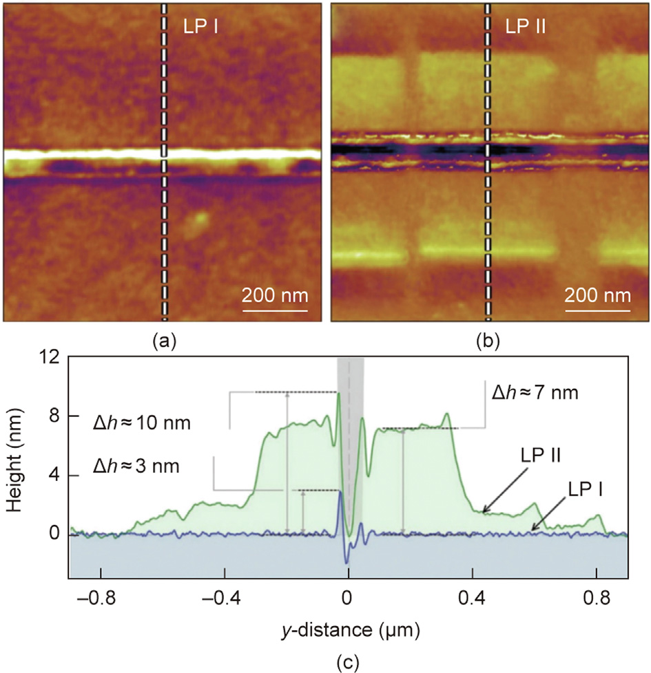
Fig. 16. AFM micrographs showing the topography of an exposed Si wafer surface after detachment of an NW. The presence of residue can be observed at the location where an interface with the NW was originally formed. (a, b) Region where high resolution SEM imaging (a) was not undertaken and (b) was undertaken. (c) Crosssection line profiles taken from locations as demarcated in the micrographs. LP: line-profiles;  : maximum residue height. Reproduced from Ref. [15] with permission.
The AFM examination carried out by Mead et al. [15] highlights how the EM environment can significantly alter the condition of a 1D interface. A 1D material examined within an EM therefore exhibits different adhesive behavior as to when in ambient conditions. When a 1D interface is formed in an ambient environment, the adjacent surfaces of the interface components are partially separated by water molecules in the form of capillary bridges [225]. The vdW forces associated with the atoms of each surface act across this medium [226]. When inducing separation of the interfacial, mechanical work must be done to overcome both the vdW interactions and the capillary forces. Under vacuum there are no capillary forces due to the vaporization of water molecules. The absence of a water medium between the interface surfaces also alters the vdW interactions [227]. Some 1D materials, including ZnO NWs, exhibit polar surfaces [228]. The polar nature of ZnO may also induce polarization of the substrate. For example, a Si surface is polarizable [229]. Consequently, electrostatic interactions may act across a 1D interface in both an ambient and EM environment. During imaging in an EM, a 1D material is irradiated with electrons. If the 1D material is not grounded (for example, when the 1D material is not in contact with the substrate, or when the 1D material is in contact with the substrate but either the interface or the substrate is not conductive), then a charge buildup can occur. For example, a Schottky barrier was expected to be present at the ZnO NW–Si substrate interface investigated by Mead et al. [15]. Thus, electrostatic interactions have the potential to be further enhanced by the EB within an EM. The potential for EB induced electrostatic interactions to alter nanoscale adhesion is also explored in other studies [230,231]. Within an SEM chamber, the low energy EB may have sufficient energy to induce hydrogen bonding is some interfacial systems [232]. Within a TEM chamber—where larger acceleration voltages are utilized—there is a greater potential for the EB to modify chemical bonds within the vicinity of a 1D interface. For example, EB acceleration voltages as low as 80 keV can produce a momentum that exceeds the binding energy of a C–C bond, permitting the displacement and recombination of C atoms. This process—known as ‘‘knock-on damage”— can introduce lattice defects into carbon-based nanostructures, including CNTs [132,233].
It is clear that a large variety of mechanisms are available within the EM environment to modify 1D interfaces, and hence alter the interfacial adhesion of 1D materials. A number of these mechanisms can ultimately be considered responsible for the earlier discussed discrepancy between the interfacial adhesion energies obtain by Mead et al. [15,76] in 2018 (MS #21) and in 2020 (MS #4). The ZnO NW–Si substrate interfacial adhesion energy obtained by Mead et al. [76] in an ambient environment can therefore be considered to provide a better representation of in-device adhesive behavior. Recognizing the critical role of the testing environment, future researchers are expected to focus on characterization methods that can investigate 1D adhesion under carefully controlled environmental conditions.
《9. Outlook》
9. Outlook
This review emphasized that the environmental conditions to which a 1D interface is exposed during sample preparation and testing can substantially alter the adhesion behavior of the 1D material. It is therefore critical during adhesion testing to establish which interfacial interactions are present at the interface of interest in order to interpret the adhesive behavior. Thus, future investigations of 1D interfaces are expected to focus on isolating and controlling the contributions of specific interfacial interactions. Realizing this research objective requires characterization techniques with the versatility to be carried out in controllable environments. The use of SEM and TEM to provide visualization during adhesion testing will be avoided in order to prevent exposure of the 1D material of interest to a high-vacuum and EBirradiated environment. AFM- and OM-based techniques are considered to be better suited for adhesive testing; however, their respective lack of and low-resolution visualization capabilities will remain a challenge. For the fundamental study of interfacial interactions, future AFM- and OM-based techniques are expected to be carried out inside environmental chambers in which environmental conditions can be precisely controlled. This direction has already been pursued by Strus et al. [107] (MS #7) in a preliminary manner, by carrying out AFM-based testing inside a dry nitrogen environment. In such a low humidity environment, the influence of vdW interactions on the adhesion behavior of a 1D material may be isolated from that of capillary forces. This strategy is expected to be explored further, especially as AFM companies such as Bruker/JPK now offer CryoStage attachments [234]. The CryoStage could conceivably facilitate microcantilever-based force spectroscopy tests for 1D materials in controlled environmental conditions. To be specific, the CryoStage incorporates a heater, liquid nitrogen supply, and can be purged with nitrogen, therefore provides temperature and relative humidity control. A similar strategy to that of Strus et al. [107] was employed by Yu et al. [235,236] in 2019 and 2020 in order to systematically investigate the environmental-dependent adhesion of mica nanolayers. In this case, testing was carried out in a glovebox, where the relative humidity and temperature were carefully controlled. A complex relationship between temperature, relative humidity, and adhesion was observed. The optical interferometric-based mica bridge method utilized by Yu et al. [235,236] is similar to the NW arch method presented by Mead et al. [76] (MS #4); therefore, the same glovebox setup could theoretically be applied to the study of the environmental-dependent adhesion of NWs. In this direction, Yibibulla et al. [188] in 2022 utilized OM in combination with a custom glovebox to investigate the influence of relative humidity on the shearing behavior of NW pairs. We therefore expect that future investigations of NW adhesion will be carried out using OM inside environmental chambers. The most commonly explored NW interfacial configuration thus far is that between an NW and a substrate. However, as research into biomimetic adhesives and sensors that exploit arrays of 1D materials has expanded, the interactions between NW pairs or between NWs in an array have become particularly relevant. The authors therefore expect that future studies will investigate NW–NW interactions in more detail, expanding further on the recent work by Yibibulla et al. [188].
Furthermore, as has been briefly discussed elsewhere [27], we consider that NWs have the untapped potential to be used more generally as adhesion force sensing probes. In the context of an force sensing probe, an NW can take the role of the ‘‘probe tip” (analogous the pyramidal tip of an microcantilever) by establishing adhesive contact with the sample surface of interest. The NW can simultaneously also act as the ‘‘deflecting component” of the probe (analogous to main cantilever beam of microcantilever) where its deflection—induced by adhesive forces—can be readout from OM micrographs or using interferometric methods [237,238]. In this way, an NW adhesion probe could conceivably be used to scan and hence map the surface of samples with complex geometry, thereby providing a unique alternative to the existing adhesion mapping capabilities provided by current top–down-fabricated microcantilever technologies [239]. Taking this idea further, an efficient OM-based readout approach could be achieved by using machine-vision to automatically extract the deflection profile of an NW from a series of micrographs [240–242]. The development of such a tool will rely on researchers possessing a full understanding of the deformation behavior of an NW when brought into contact with an substrate.
Recent progress has also been made toward the surface modification of CNTs that are used as an interphase in composite materials for the purpose of enhancing the mechanical performance of the final composite [65]. This approach, which is also referred to as ‘‘molecular engineering,” involves the chemical bonding of ‘‘binding” molecules to the surface of CNTs in order to functionalize them and promote further bonding to the polymeric material of the matrix phase. We consider that future research will endeavor to reliably ‘‘tune” the adhesion behavior of 1D materials through their surface modification. This could be done by chemical means, as has been explored in composite science, or by physical means, through the controlled inclusion of surface defects or surface roughness.
《Acknowledgments》
Acknowledgments
This project was financially supported by the German Research Foundation (509134333), the Australian Research Council (DP220103222), and the National Natural Science Foundation of China (11674399).
《Compliance with ethics guidelines》
Compliance with ethics guidelines
James L. Mead, Shiliang Wang, Sören Zimmermann, Sergej Fatikow, and Han Huang declare that they have no conflict of interest or financial conflicts to disclose.


 京公网安备 11010502051620号


