

《1. Introduction》
1. Introduction
According to the Merriam–Webster dictionary, the definition of ‘‘embed” is ‘‘to make something an integral part of” [1]; thus, ‘‘embedded cooling” broadly encompasses cooling technologies located directly on or inside an active electronic device (e.g., a microprocessor or power electronic device). Embedded cooling strategies can employ purely conduction heat transfer [2–4], single-phase forced convection [5–7], two-phase forced convection [8], natural convection (single or two-phase) [2], immersion cooling [9,10], heat pipes or vapor chambers [11–13], active refrigeration [14,15], or phase-change cooling [16,17]. Bringing the cooling closer to an active device is becoming ever more necessary due to the increased heat fluxes in microprocessors and power electronics, as well as the increasing packing densities of devices and their shrinking form factors. In terms of these trends, microprocessor computational power is hitting thermal limits due to the exponential growth in heat dissipation that coincides with Moore’s Law [18]. As a result, thermal considerations are creating a bottleneck in the advancement of microprocessor cores. There is also a developing trend to co-locate multiple devices within a package, in what is called heterogeneous integration (HI) or three-dimensional integrated circuits (3DICs) [19]. Tighter electronics packing means faster communication and computation, which is especially important in high-performance computing. These trends are pushing high heat flux packages closer together, meaning that conventional lateral spreading is becoming increasingly difficult due to the tight spatial integration of circuitry [20]. In power electronics, extreme heat fluxes are possible, causing new strategies to be needed (e.g., 30 kW·cm–2 at the transistor and at least 1 kW·cm–2 at the die) [21]. Embedded cooling provides an advantage in addressing high heat fluxes by eliminating thermal interface materials (TIMs) that would otherwise increase the resistance and hurt the thermal budget.
《Fig. 1》

Fig. 1. An overview of the wide variety of embedded cooling technologies [22].
The architectures of embedded cooling technologies have a plethora of forms, as shown in Fig. 1 [22]. The general hierarchy includes conduction-based and convection-based technologies. Conduction-based technologies encompass high thermal conductivity films (e.g., chemical vapor deposition (CVD) diamond) for near-junction heat spreading, thermal vias made of copper to transport heat vertically through a chip, and thermoelectric devices to actively cool devices. Convection-based embedded cooling technologies typically employ fluid-directing structures on top of or inside the active electronic device (i.e., inter-chip or intra-chip cooling) and extended surfaces. Such convection-based embedded cooling devices have primarily been made from etched microchannels produced on microfabricated dies. More recently, printed metal fins are being explored as freeform metal cooling structures constructed directly on active electronic devices [23–26]. These strategies are introduced further below and discussed in depth in Section 2.
Passive embedded cooling strategies enhance conduction heat transfer within the chip by employing high thermal conductivity materials that help lower the thermal resistance. One method is to add thermal vias going vertically and thermal interconnects going laterally that can serve as a thermal pathway and, potentially, as an electrical signal pathway. Since copper has a much greater conductivity than the traditional dielectrics used in microprocessors (0.1–1.0 W·m–1 ·K–1 ), increasing the density of copper in the interconnect layer, beyond the electrical signal requirements, increases the thermal performance. Conduction-based thermal-management strategies include through-silicon vias that conduct heat vertically over hot spots [4] and the coating of active layers in high thermal conductivity materials such as diamond [2,27] or pyrolytic graphite [28].
Convective embedded cooling technologies, such as etched silicon microchannels [17,29] and metal three-dimensional (3D)- printed cooling fins [23–26], directly attach to the active device. Etched silicon microchannel-based technologies have been investigated the most, although alternative technologies such as printing metal fins onto silicon are also being examined. The coolant choice and whether that fluid operates in single- or two-phase convection are important considerations. Two-phase cooling can operate with small temperature differences, even when cooling multiple devices in series, due to the large latent heat of many fluids. Designers must operate below critical heat fluxes, as abrupt failures occur if these are exceeded. Water has excellent heat capacity and latent heat, and has been safely used for electronic cooling with robust plumbing solutions, such as the International Business Machines (IBM) Corporation mainframe ZEnterprise 196. However, water cannot come into contact with active electronic circuits and is still viewed as risky by some end users, so various dielectric fluids have also been explored, such as Novec and mineral oil. These dielectric fluids are more expensive than water and often possess less desirable heat-dissipating properties (i.e., thermal conductivity, specific heat, latent heat, and critical boiling heat flux), but they are electrically insulating. A full comparison of fluids for forced convection, natural convection, and two-phase convection (pool boiling and flow boiling) is provided in Section 3.
General challenges of embedded cooling technologies that have limited their widespread adoption include their perceived complexity and expense, the high-level coordination required between electrical circuit and thermal engineers, new manufacturing processes, reliability risks, yield reduction, restricted re-workability, and supply-chain risks. These challenges—whether real or only perceived—have limited the adoption of many embedded cooling technologies; however, there is growing consensus that such technologies are on the critical path to advancing electrical performance. The following section examines the scaling limits of embedded cooling for different cooling, heat spreading, and fluid combinations and discusses the challenges and opportunities of convective cooling technologies in microfabricated etched die channels and 3D-printed fins.
The traditionally employed thermal-management solution is a remote separable cold plate/heat sink indirectly attached to the heat source or chip with a TIM, as shown in Fig. 2. Thermalmanagement technologies for electronic packages can generally be classified as follows:
• T1 (Technology 1): directly embedding the cooling solution on the chip;
• T2 (Technology 2): directly embedding the cooling solution on the lid;
• T3 (Technology 3): advanced heat spreaders (vapor chamber/ heat pipe);
• T4 (Technology 4): traditionally attached heat sink/cold plate.
《Fig. 2》
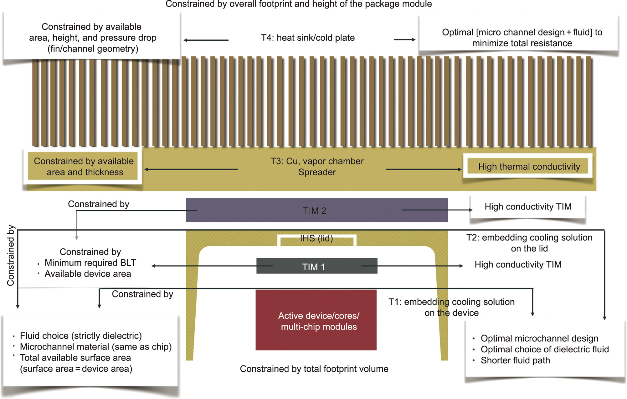
Fig. 2. Schematic of cooling technologies at different levels, ranging from on-device to cold plate/heatsinks. Also listed are various optimization opportunities at each technology level (T1–T4), with objectives on the right side and constraints on the left side. TIM 1 refers to the TIM between the active die and the lid or integrated heat spreader (IHS). TIM 2 refers to the TIM between lid and the cold plate heat spreader. BLT: bond line thickness; T1: Technology 1; T2: Technology 2; T3: Technology 3; T4: Technology 4.
The most pragmatic and reliable thermal-management solution for today’s electronic packages is to employ parallel channel heat sinks/cold plates that are separately attached to the device (T4). Such solutions take the form of either air cooling or liquid cooling. Both air and liquid cooling offer many advantages and challenges. The main advantage of an air-cooled heat sink is that it is the most reliable cooling technology. However, the inferior heat transfer properties of air impede the thermal transport and often demand bulk heat sink design to offer enough surface area for heat exchange. In addition to the large heat sink design required for air cooling, heat pipes and vapor chambers are employed to effectively move and spread the heat from a small chip area.
Liquid-cooled heat sinks provide compact, high heat transfer thermal-management solutions with superior heat transport capabilities. However, liquid-cooled heat sinks are often prone to leakages, due to their high-pressure operation. Moreover, the inferior dielectric properties of water impede the implementation of liquid water close to a chip (active electrical circuit). Tuckerman and Pease [30] embedded the liquid cooling solution directly onto the silicon; by doing so, they demonstrated a high heat flux removal of 790 W·cm–2 with a silicon temperature rise of 71 °C. Although this work is attractive from a heat transfer perspective, the technical challenges associated with the implementation of such a technology were not considered or discussed.
The existing limits of air- and liquid-cooled heat sinks are 55 and 175 W·cm–2 . Future heat flux and chip size trends will pose more significant challenges for air- and liquid-cooled heat sinks (T4). The TIM between lid and the cold plate heat spreader (TIM 2) and spreading resistance contribute significantly in the overall resistance from chip to coolant. Advanced thermal-management technologies (T3) such as high-conducting TIM and vapor chamber heat spreaders are required to sustain the use of a thermal solution involving separable cold plates. Otherwise, such technologies are often limited by the maximum heat flux, especially with growing hotspots (i.e., regions of localized high heat fluxes).
To augment the heat flux limits, embedded cooling is an attractive technology. In this article, we aim to review and compare three possible embedded cooling technologies: etched microchannel within the device, printed fins on the device, and immersion cooling via pool boiling. Fig. 3 [5,7,17,22,30–38] establishes the regime map for different chip sizes, microchannel design concepts, and coolants from the recent embedded cooling literature. It should be noted that Fig. 3 pertains only to chips with uniform heat flux. Future concepts must focus on lower temperature operation at higher heat fluxes through a smart choice of coolant, microchannel design, and shorter fluid paths to lower caloric resistance. A shorter fluid path enables local heat removal, thereby eliminating the caloric resistance of the cold plate resistance, as demonstrated by Drummond et al. [38].
《Fig. 3》
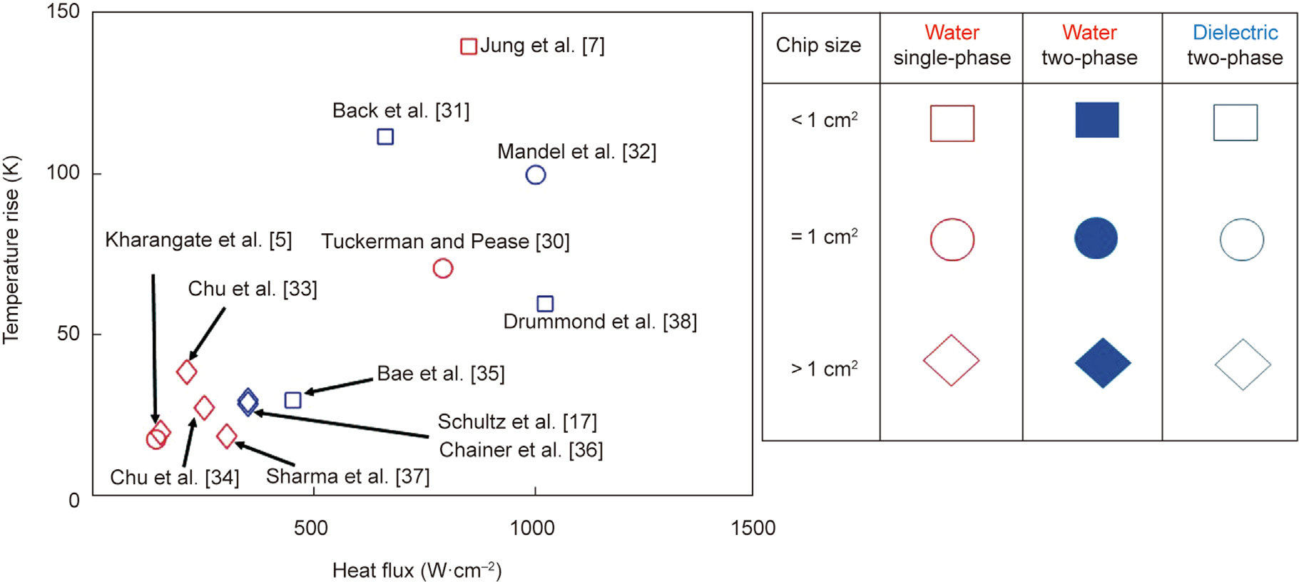
Fig. 3. Regime map of recent advancements in embedded cooling trends [22]. This figure excludes 3D-printed fins; the latter is discussed later in Sections 4.2 and 4.3.
《2. Scaling limits for convective embedded cooling versus nonembedded cooling》
2. Scaling limits for convective embedded cooling versus nonembedded cooling
The tradeoff between employing embedded cooling (T1 and T2 in Fig. 2) or employing a bulky non-embedded cooling solution (i.e., a heat spreader/lid combined with a heat sink; T3 and T4 in Fig. 2) must be studied in order to understand the challenges of transitioning to direct embedded cooling. The overall thermal resistance can be deconstructed into the resistance due to the spreader and the resistance due to the heat sink. These two resistances have conflicting trends with the area ratio (AR)—that is, the ratio of the spreader area to the chip area. AR is defined as AR = As/Ac, where As is the spreader area and Ac is the chip area/size.
The convection resistance of the heat sink decreases with the AR, while the spreading resistance increases. We will examine the total thermal resistance for air cooling and then water cooling. Subsequently, we will study how a thicker high-conductivity electronic die can improve heat dissipation from hotspots.
The analytical solutions provided by Shah and London [39] and Zhang et al. [6] were employed to calculate the heat sink resistance for developing-to-developed flow through parallel microchannel, as shown in Fig. 4. The spreading resistance was modeled using the approximate analytical solutions of Song et al. [40].
Total resistance of heat sink = conduction resistance + convection resistance + caloric resistance (1)
Total resistance of the spreader = direct one-dimensional conduction resistance + spreading resistance
In the forthcoming discussions, the spreading resistance refers to only the spreading component of the total spreading resistance, exclusive of the direct one-dimensional (1D) conduction resistance.
The parameter values for calculating the different components of the resistance for air cooling are Ac = 1 cm2 , air velocity (Vair) = 10 m·s–1 , channel width (wch) = 1 mm, fin/channel height (hch) = 25 mm, spreader thickness (ts) = 10 mm, spreader conductivity = 150 W·m–1 ·K–1 .
The parameter values for calculating the different components of the resistance for liquid cooling are Ac = 1 cm2 , volume flow rate (Q) = 0.5 L·m–1 , wch = 0.05 mm, hch = 0.3 mm, ts = 10 mm, spreader conductivity = 150 W·m–1·K–1 .
《Fig. 4》

Fig. 4. The heat sink and flow configuration employed for calculating various components of the resistance for air and liquid cooling. All of the top and side walls are adiabatic. Uniform heating for AR = 1; localized heating (at the center of the base) for AR > 1. wch: the channel width; hch: the channel height; ts: the spreader thickness.
As made evident by Fig. 5 [22], the enhancement in area reduces the convection resistance while increasing the spreading resistance within the discussed resistance decomposition framework. In Fig. 5 [22] the case where AR = 1 pertains to embedded cooling, as the cooling area is the same as the available chip area. As the AR increases to greater than 1, the case corresponds to nonembedded cooling, as the chip area is not equal to the cooling surface area. For such cases, the spreading resistance increases. A common method to reduce the spreading resistance is to employ heat pipes and vapor chambers. The general vapor chamber resistance range is shown as a shaded grey region on the plot [12]. Another factor is that, whenever non-embedded cooling (AR > 1) is used, an additional conduction resistance from TIM 1 (the TIM between active and lid) is added but is not accounted for in these values. With AR > 1, the junction temperature is determined by the sum of the heat sink resistance, the spreader resistance, and the TIM 1 resistance. An adequately designed air-cooled heat sink can have a thermal resistance as low as 0.25 K·W–1 for AR > 30 and an active area of 1 cm2 , excluding spreading and TIM resistance. The total external resistance, including heat sink and spreading resistance, is estimated to be 0.5 K·W–1 . The total external resistance could be further minimized by using a vapor chamber heat spreader. However, a directly air-cooled heat sink with AR = 1 has a resistance greater than 2.5 K·W–1 , making it clear that direct air cooling is not a feasible solution, even for modest heat loads.
《Fig. 5》

Fig. 5. Variation of the resistance components of an air-cooled heat sink with an area enhancement ratio. The details of the model parameters are: Ac = 1 cm2 ; heat sink and spreader conductivity = 150 W·m–1 ·K–1 ; ts = 10 mm; wch = 1 mm; hch = 25 mm; Vair = 10 m·s–1 [22]. This figure excludes the TIM resistance. The grey region indicates the thermal resistance of the vapor chamber heat spreader [12].
The resistance for a liquid cold plate versus the area enhancement ratio is shown in Fig. 6 [22]. Liquid-cooled cold plates take advantage of the high heat transfer coefficient in the microchannel. Therefore, enhancing the area leads to marginal performance benefit after an AR of about 4. Thus, a cooling solution (AR = 1 in Fig. 6 [22]) with forced liquid cooling can be beneficial and is comparable to attaching bulk separable cold plate solutions (AR > 1). Liquidcooled cold plates with no area enhancement (embedded cooling, AR = 1) can have a thermal resistance of 0.095 K·W–1 , and the total thermal resistance is just the heat sink resistance without the spreading resistance. The total external thermal resistance is only plotted for AR > 1. For AR = 1, the total external resistance is the same as the heat sink resistance shown in the plot.
《Fig. 6》

Fig. 6. Variation of the resistance components of a liquid-cooled heat sink with an area enhancement ratio. The details of the model parameters are: Ac = 1 cm2 ; heat sink and spreader conductivity = 150 W·m–1 ·K–1 ; ts = 10 mm; wch = 0.05 mm; hch = 0.3 mm; Q = 0.5 L·min–1 [22]. The plot excludes the TIM resistance. The grey region indicates the thermal resistance of the vapor chamber heat spreader [12].
In contrast, non-direct liquid cooling with an AR of 4 (nonembedded cooling) would have a lower heatsink resistance of 0.025 K·W–1 , but the total external resistance would be dominated by the sum of the resistances of the spreader (0.35 K·W–1 ) and the TIM. Importantly, this shows the benefit of embedded cooling without any spreading for liquid cooling, compared with embedded cooling with conventional spreading, which would have overall higher resistance. Printing the heat sinks directly onto silicon is an especially appealing technology, because it permits an increased convective surface area with minimum interfacial resistance [25,26]. If an unconventional spreader or spreaders utilizing phase change, such as a vapor chamber, were used, the calculations would show a smaller overall resistance than a conduction spreader, as the effective conductivity would be larger. Vapor chambers have a thermal resistance ranging from 0.03–0.35 cm2 ·K·W–1 [12]. Technologies such as direct printing could enable the interfacing of vapor chambers to chips without the use of TIMs.
Moreover, embedded cooling has several key advantages:
(1) It makes thermal management an integral part of the chip design and power delivery;
(2) It enables co-design, as the thermal design becomes a part of the chip design;
(3) It improves the functionality of the device, especially given the growing interest in HI.
As mentioned in the previous discussion, the advantages of embedded cooling are maximized when using liquid cooling. Although embedded liquid cooling is attractive from a heat transfer perspective, it also introduces some key challenges in terms of:
• Material compatibility;
• Leak-proof sealing and flow routing;
• The need to minimize interference with electrical functionalities;
• Configurability for multi-chip modules;
• Replaceability.
《3. Comparing embedded cooling fluids》
3. Comparing embedded cooling fluids
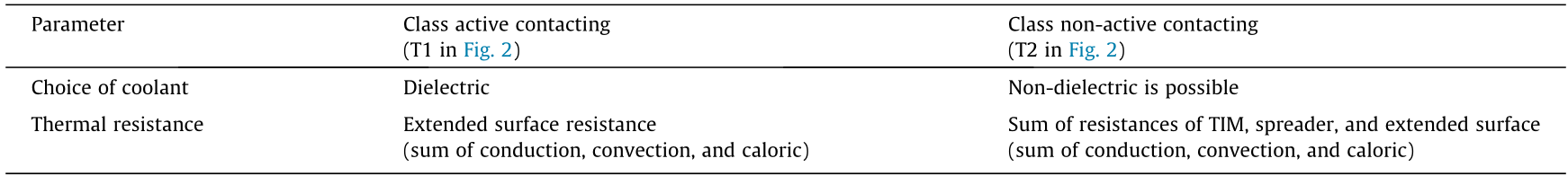
For indirect cooling with cold plates, chemical and electrical compatibility between the liquid and the electronic components is not an issue, and water—a liquid with excellent heat transfer properties—may be employed. In the case of indirect cooling, where the fluid does not directly come into contact with active devices, stringent constraints on the electrical properties of the fluid are not required (class non-active contacting). However, for embedded cooling in which the fluid comes into contact with powered active devices, as shown in Fig. 7, stringent chemical and electrical requirements are imposed on the liquid (class active contacting). Opportunities to maximize heat transfer in different classes of embedded cooling are shown in Fig. 7. The constraints for optimal fluid selection depend upon the class of embedded cooling and the liquid’s chemical and electrical properties, as shown in Table 1. For compatibility with the chip substrate and printed circuit board materials, such as printed wiring boards, silicone, and plastic materials, the liquid must be chemically inert and non-absorbable by these materials. Furthermore, electrical isolation must be provided between closely spaced conductors. Desirable properties for a fluid for embedded cooling include stability, nontoxicity, nonflammability, inertness, a high dielectric strength, and a low environmental impact (i.e., non-ozone depleting, low global warming potential (GWP), and eventually decomposes after accidental release).
《Fig. 7》
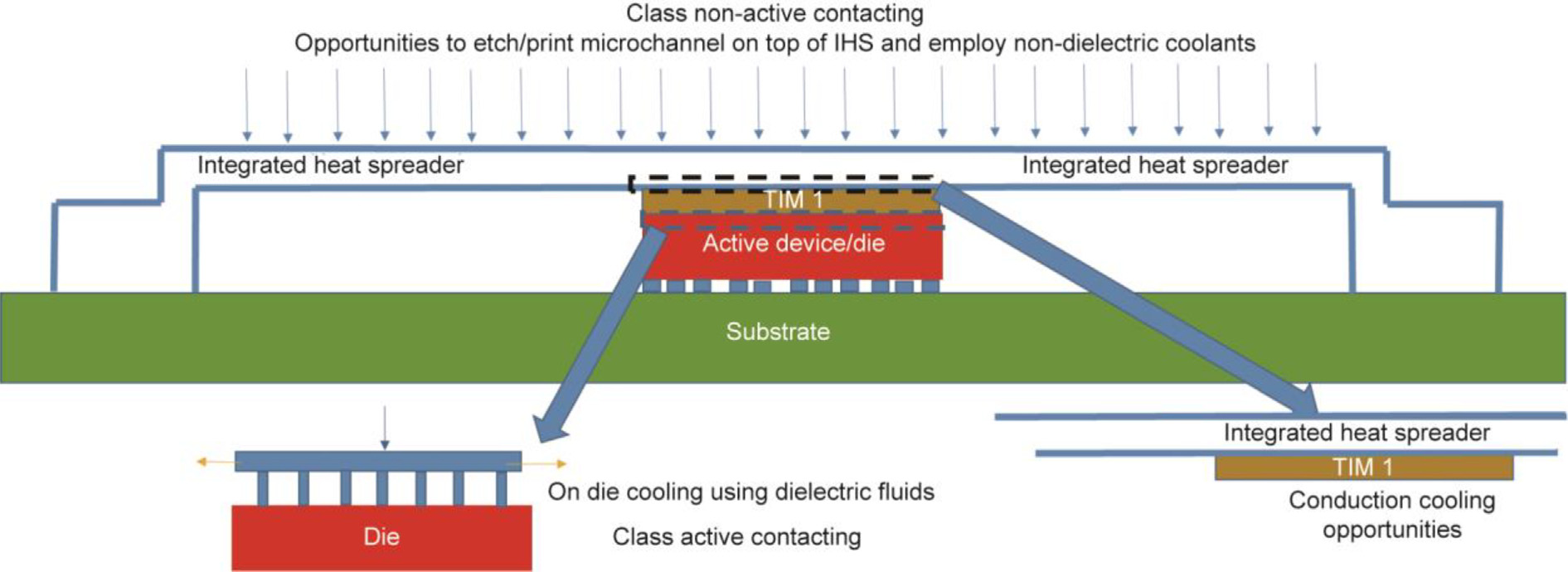
Fig. 7. Opportunities in embedded cooling over a die/chip module.
《Table 1》
Table 1 Different classes of embedded cooling and associated descriptions.
Fluid selection for embedded cooling can be posed as an optimization problem with the objective of maximizing heat transfer for the minimum junction temperature rise, subject to maximum reliability and good material compatibility. The constraints for implementing an embedded technology in a practical application are shown in Fig. 8 [22].
《Fig. 8》

Fig. 8. Constraints on embedded cooling technology [22].
A variety of coolants are available with superior thermal properties that could be attractive from a heat transfer perspective. However, their dielectric properties restrict the implementation of such coolants in close proximity to the heat generating devices. For example, water has excellent thermophysical properties but is often inhibited by its dielectric properties in the implementation of embedded cooling or immersion cooling. Fluorocarbons (FCs) such as FC-72, FC-86, and FC-77 are generally employed for on-chip cooling. Although FCs, such as the family of Freons, present serious environmental problems that make them unsuitable choices due to their high GWP and ozone-depletion capacity, we include them in the discussion as a point of comparison for more environmentally benign coolants, such as hydrofluoroethers (HFEs). Table 2 provides a comparison of the thermal properties of commonly employed coolants in embedded cooling.
《Table 2》
Table 2 Comparison of the thermophysical properties of the three most commonly used coolants for embedded cooling.

cSt: centistokes; 1 atm = 101 325 Pa.
Fig. 9 [22] establishes the tradeoffs in the thermal and electrical properties of three main class of coolants employed in embedded cooling. Liquid water is highly desirable due to its heat transfer, but the risk associated with circuit contact makes it undesirable for active contacting embedded cooling. A recent study from Birbarah et al. [9] demonstrated a proof of concept that employed liquid water for direct chip cooling by efficiently isolating the electrical circuit using conformal layers (~1 μm thick) of parylene C. This method may present serious practical difficulties once deployed on a large scale due to challenges such as material computability, short circuit as outlined in Section 2.
《Fig. 9》
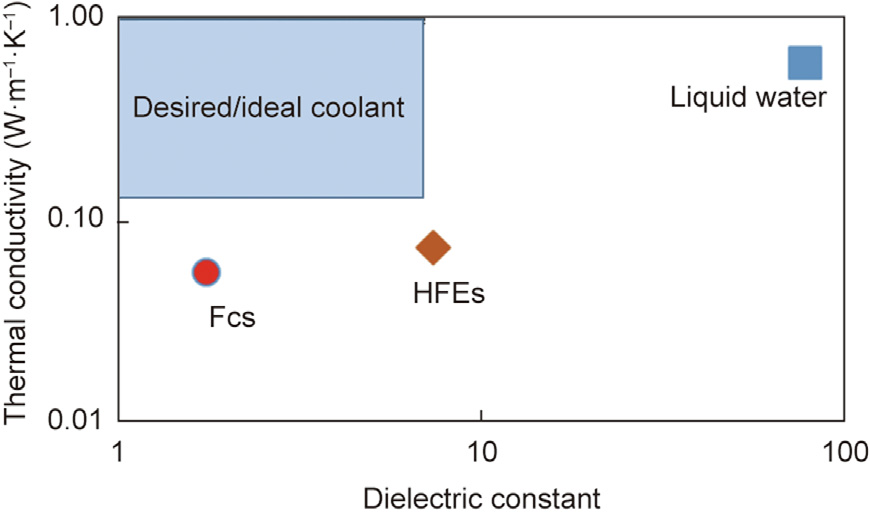
Fig. 9. The tradeoff in heat transfer and electrical properties [22] for three classes of coolants preferred for the embedded cooling of electronics.
Saylor et al. [41] developed figures of merit (FOMs) to compare the effectiveness of different fluids for different cooling modes. The discussed FOMs pertain to fluids in the temperature range of 290– 370 K. The averaged properties of fluids are employed in the calculation of FOMs. For boiling, the FOMs pertain to a pressure of 1 atm (1 atm = 101 325 Pa). Higher FOM values translate to better heat transfer performance. Below, we plot coolants according to FOMs (Eqs. (2)–(5)).
《3.1. Natural convection》
3.1. Natural convection
The following Eq. (2) is used to calculate the FOM for natural convection:
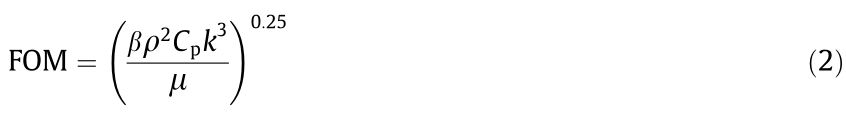
where β is the thermal coefficient of expansion, ρ is the density, Cp is the specific heat; μ is dynamic viscosity, and k is the thermal conductivity.
As far as natural convection is considered, Fig. 9 [22] clearly shows that water is best, while HFEs and FCs are significantly less preferable.
《3.2. Forced convection》
3.2. Forced convection
The following Eq. (3) is used to calculate the FOM for forced convection:

where n and m are exponents.
《3.3. Pool boiling》
3.3. Pool boiling
The following Eq. (4) is used to calculate the FOM for pool boiling:

where hfg is the heat of vaporization, σ is the surface tension, g is acceleration due to gravity, ρg is gas density, and ρf is fluid density.
《3.4. Flow boiling》
3.4. Flow boiling
The following Eq. (5) is used to calculate the FOM for flow boiling:

The FOMs in Figs. 10–13 [22] calculated from Eqs. (2)–(5) make it evident that water outperforms other coolants in terms of superior heat transfer capabilities. R-113 has a higher FOM among the dielectric fluids. Despite their attractive dielectric properties, the inherently inferior thermal properties of FC and HFE coolants pose a significant challenge to the chemical engineers involved in developing such fluids. Even though (deionized) water possesses the best thermal properties, it cannot be employed in close proximity to an active device. Recently Ref. [42], R134a and R245fa have been demonstrated to exhibit optimal heat transfer performance among the dielectric coolants.
《Fig. 10》

Fig. 10. FOM for coolants employed in natural convection [22]. WEG: water ethylene glycol.
《Fig. 11》
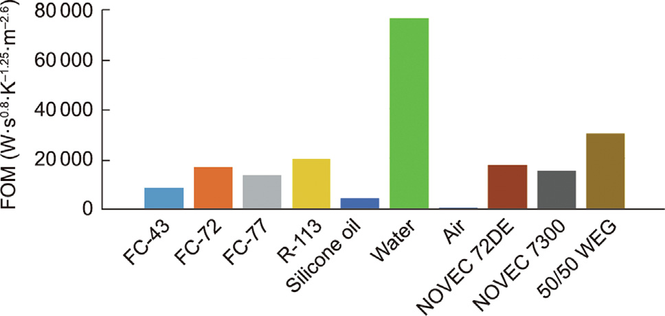
Fig. 11. FOM for coolants employed in forced convection [22].
《Fig. 12》
Fig. 12. FOM for coolants employed in immersion pool boiling [22].
《Fig. 13》
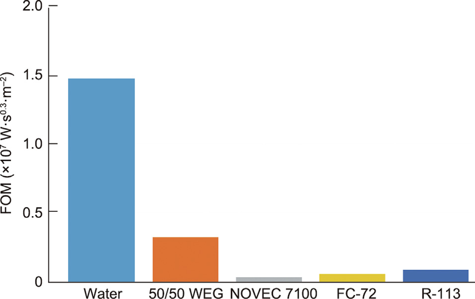
Fig. 13. FOM for coolants employed in embedded flow boiling [22].
Liquid metals [43] are emerging as an attractive option for cooling high-power dissipating electronics. An exciting study by Xiang et al. [43] demonstrated the efficiency of employing liquid metals for the jet impingement cooling of high-power electronics, in comparison with liquid water. The researchers achieved a very low thermal resistance of 0.033 K·W–1 utilizing liquid gallium. However, the material compatibility of employing liquid metals as an option for on-chip embedded cooling requires further investigation for pragmatic applications.
《4. Embedded cooling solutions》
4. Embedded cooling solutions
《4.1. Etched electronic substrate-based embedded cooling solutions》
4.1. Etched electronic substrate-based embedded cooling solutions
Etched electronic technologies can utilize single- or two-phase systems. Various geometries have been explored, including parallel microchannels [44], radial channels with fins [17,29], impinging jets [45], and nano-membrane evaporation [8]. The first published discussions of etched silicon microchannels occurred in the late 1970 s and early 1980s [30,46].
The seminal work of Tuckerman and Pease [30] demonstrated a thermal resistance of 0.09 cm2 ·K·W–1 over a 1 cm2 surface area for fins 50 μm in separation and width and 300 μm in height, when operating under uniform heat fluxes of up to 790 W·cm–2 with water as the working fluid (a maximum pressure drop of 31 pounds per square inch (psi) or 213 kPa). The fluid entered and exited manifolds in the etched silicon fin array via holes in the glass cover. Saylor et al. [41] numerically demonstrated that, by bringing the coolant closer to the semiconductor die, a hotspot heat flux of 1 kW·cm–2 could be managed thermally. Saylor et al. [41] also discussed the viability of different cooling techniques such as jet impingement cooling and spray cooling, and their associated thermal limits. Readers interested in the thermal limits of various cooling technologies are referred to the HI roadmap chapter namely single and multi-chip module in Ref. [47]. Furthermore, interesting work on modular micro-convective cooling via jet impingement directly on a multi-chip module surface has been demonstrated by May et al. [48].
The researchers demonstrated hotspot-targeted jet impingement on a TIM in a direct-to-die or direct-to-package technology with an attractive junction-to-fluid thermal resistance of 0.15 K·W–1 .
Alternate fluids and designs have been studied since the work of Tuckerman and Pease [30] IBM demonstrated a two-phase radial microchannel solution using the refrigerant R1234ze [29]. This system had a critical heat flux of 340 W·cm–2 and a low standard deviation between measured temperature values on the chip (4.5 °C). The thermal resistance just below this critical heat flux was 0.09 cm2 ·K·W–1 at 120 kPa [17]. It is noteworthy that the critical heat flux for this two-phase device was less than the heat flux demonstrated for single-phase water by Tuckerman and Pease [30] while the thermal resistance was approximately the same. Many cryo-refrigerants have relatively low critical heat fluxes compared with water, due to their lower heat of vaporization and weaker surface tension. The flow boiling critical heat flux can be increased by increasing the refrigerant flow rate.
Two-phase jet impingement cooling sprays a fine mist of fluid impinging onto a hot surface, which creates a thin fluid film that cools via a combination of convection and evaporation at low superheats (Tw – Tsat < 15 °C, where Tw is wall temperature and Tsat is saturation temperature) and via boiling at higher superheats [45]. The benefits of spray cooling include low superheats and the ability to carry high heat fluxes before exceeding a critical heat flux, as well as the ability to multiplex many spray nozzles above one surface. The disadvantages of spray cooling include relatively high pressure drops across nozzles (e.g., 70–300 kPa, typically), the fouling potential of small nozzle openings, and diminished performance when non-condensable gases enter the system. The thermal resistances and critical heat fluxes are 0.10–0.12 cm2 ·K·W–1 and 525–945 W·cm–2 for water [49], 0.16–0.21 cm2 ·K·W–1 and 357–490 W·cm–2 for methanol, 0.45–0.60 cm2 ·K·W–1 and 65–83 W·cm–2 for FC-72, and 0.49–0.63 cm2 ·K·W–1 and 79–90 W·cm–2 for FC-87, where the range represents variation due to the operating pressure difference and other conditions (i.e., nozzle separation to surface, flow rate, nozzle design, and mean spray diameter) [45].
Evaporative cooling with nanoporous membranes (600 nm thick, pore diameter Φ < 140 nm) was recently demonstrated to provide device-level thermal resistances and critical heat fluxes of 0.15 cm2 ·K·W–1 and 144 W·cm–2 for water, and 0.055 cm2 ·K·W–1 and 550 W·cm–2 for pentane [8,50]. In this work, a network of channels was created to support fluid replenishment into nanoscale pores, through which evaporative cooling proceeded. The work also demonstrated ultra-high heat fluxes through individual pores (up to 2.7 kW·cm–2 ), and affirmed the findings from a study of individual nanopores [51]. The reliability of this new kind of device needs further study, as non-volatile contaminants accumulated in the pores, degrading the performance after a relatively short period of time [50].
Silicon microchannels with a high AR can be achieved in several ways; for a detailed manufacturing discussion, interested readers are referred to Kandlikar and Grande [52]. Tuckerman and Pease [30] used anisotropic wet chemical etching (KOH). This process proceeds at an etch rate of about a micron per minute, so the etching time required for heat-removal devices is on the order of hours. Moreover, anisotropic etchants require consideration of the substrate crystal orientation, as the crystals act as etch stops. Anisotropic etching can also be done via deep reactive ion etching (DRIE), which uses alternating cycles of etching and polymeric passivation. Typical DRIE rates of up to 40 μm·min–1 are possible with specialized tools, although rates of 2–8 μm·min–1 are more typical. However, industrial manufacturers are reluctant to etch onto active devices, since concerns exist regarding reducing the device yield, so an additional bonding step onto the active device is thought to be necessary for adoption [29].
Recent development trends in embedded on-chip cooling have high heat flux targets. More recently, Rajan et al. [53] demonstrated an embedded cooling solution involving the etching of silicon as a part of the thermal management of high-power electronics. Their study showed that microfluidic cooling over etched pin fins can result in a meager thermal resistance of 0.197 °C·W–1 in a chip area of 1.5 cm2 . The researchers demonstrated that the embedded cooling technology could dissipate up to 200 W·cm–2 of localized heat flux.
Serious effort was put into developing an enhanced cooling solution by embedding the cooling solution inside the chip (intra-chip cooling) under the leadership of Bar-Cohen et al. [54] during 2012–2015. The work targeted the development of embedded cooling technology to achieve a hotspot heat flux of 5 kW·cm–2 . Their paper also summarizes the five key academic efforts made to meet the specified targets. Woodcock et al. [55] demonstrated an ultra-high heat flux removal of 1 kW·cm–2 (chip size 3.95 mm2 ) by using the flow boiling of HFE-7000 over Gen 3 Piranha Pin Fins (PPF) embedded onto the device. Nasr et al. [56] demonstrated the removal of very high heat fluxes in the range of 4.7 kW·cm–2 by the flow boiling of R134a in ultra-small microgaps. The achieved value was close to the program’s target of 5 kW·cm–2 . The researchers reported that the exit vapor quality was approaching unity. Mandel et al. [32] demonstrated the embedded two-phase cooling of high heat flux electronics in excess of 1 kW·cm–2 by employing a manifold microchannel-based fluid delivery system that was pressfitted on the silicon. Back et al. [31] demonstrated a manifold microchannel etched onto silicon to enable flow boiling through channels and demonstrated a heat flux of 660 W·cm–2 . The researchers employed HFE-7100 as the fluid and concluded that the majority of the pressure drop occurs through the manifold rather than in the microchannel.
《4.2. Additive manufacturing-based embedded cooling solutions》
4.2. Additive manufacturing-based embedded cooling solutions
While embedded cooling via silicon etching has demonstrated noteworthy cooling capabilities [17,29], alternative 3D-printed embedded cooling strategies have also begun to be explored in the literature. Techniques for printing onto electronic substrates to build cooling devices have had several architectures to date: selective laser melting using an interlayer alloy [23–26], melting metal onto a physical-vapor-deposited film [57–61], and printing thermoelectric cooling devices onto hot spots [14,15].
Silicon has many advantages as a heatsink material, as its processing enables fine features and silicon-to-silicon direct bonding can be used; however, its use also presents challenges, as the backside of an actual silicon device is unlikely to be micromachined due to poor yield, other materials have higher thermal conductivity than silicon, and building high-AR features with silicon microfabrication is challenging and time consuming. This is why prototype microchannel cooling devices have been made on a separate chip and then solder bonded to the device [51]. These challenges are motivating factors in the recent interest in printed embedded cooling features (e.g., fins, channels, and thermoelectrics).
Direct fabrication of cooling features by means of metal printing is appealing due to the freeform nature of the manufacturing process. As seen in the nascent literature on additively manufactured heat sinks, the relatively unconstrained printing process can offer performance advantages that optimize cooling for hot spots. In terms of electronics cooling, removing the interface for cooling can reduce the significant temperature drops across typical TIMs. Even relatively high-performing solid metal TIMs can have resistances on the order of 0.2 cm2 ·K·W–1 . When this is installed directly over next-generation microprocessor hot spots that will be roughly 1000 W·cm–2 , the thermal budget is exceeded just in the first chip–lid TIM (TIM 1). Even the highest performing liquid metal TIMs with datasheets showing day-zero resistances of 0.025 cm2 ·K·W–1 would consume 25 °C of the thermal budget just in the chip-to-lid TIM for intense hotspots without spreading, leaving little thermal budget from the lid to the liquid coolant, considering a typical overall thermal budget of 40–60 °C in the case of chiller-less liquid or two-phase cooling.
One study demonstrated that micro fins can be laser printed onto a silicon device. The manufacturing process involves printing a low-melting-point brazing alloy that rapidly forms silicide bonds with silicon and subsequently printing a high thermal conductivity metal on top [62]. While the brazing bonding layer has comparable thermal conductivity to solder, albeit potentially thinner, subsequent layers can be made of high thermal conductivity metals such as Cu, Ag, or Al. The manufacturing technique of direct metal printing has the potential to create very thin intermetallic-like bonding layers (e.g., titanium silicides of < 100 nm) due to the rapid laser processing conditions that limit diffusion times. Printing onto silicon and graphite has been demonstrated [23,24]. Another method uses a thick metalized interlayer that is deposited via physical vapor [57–59].
Fig. 14 shows recent research efforts on the direct printing of micro pin fins onto silicon. Conventional metal laser printers have resolution limits on the order of 200 μm due to laser sizes and metal powder dimensions. However, research has demonstrated that metals can be printed via selective laser sintering at resolutions of 1–5 μm [63,64]. As shown by these studies, the materials developed for macro-printing onto silicon can be applied to finer resolution printers that deposit thin layers of nanoparticle inks (1.5 μm wet film), dry the inks (500 nm dry film), and then laser expose the desired pattern, where the nanoparticle inks are composed of appropriate alloys. The film is then laser sintered with a beam expanded laser that selectively heats the surface via a digital micromirror array. A continuous wave or nanosecond laser can alternatively be used. The substrates used in these experiments were aluminum and glass, and the ability to build structures as tall as 7 μm with a thickness of 50 μm was demonstrated.
《Fig. 14》

Fig. 14. Printing high-aspect-ratio pin fins onto silicon (diameter 200 μm).
While conventional metal microchannel designs [65] could be made via additive manufacturing, such designs would not capture the freeform features unique to additive manufacturing. Simulations of potential designs made via direct metal printing indicate that pin–fin-type structures used in a single phase with water can have a thermal resistance of less than 0.03 K·W–1 (calculated based on the maximum die temperature and a die size of 4 cm2 ) [26]. This design is not yet fully optimized, and significant reductions in thermal resistance are anticipated in future design iterations. Another application of additive manufacturing is in the ability to fabricate manifolds for cold plate [66].
Although these technologies are appealing due to their higher performance, better customization, and greater thermal conductivity in comparison with silicon etched fins, more research is required to demonstrate the technologies, determine a scalable manufacturing strategy, and demonstrate lifetime reliability.
The thermal conductivities of the materials commonly used in electronics vary by four orders of magnitude, from a relatively low thermal conductivity of around 0.1 W·m–1 ·K–1 for many polymers and glasses, to 400 W·m–1 ·K–1 for Ag. Exceptional thermal conductors, such as natural diamond and pyrolytic graphite, which have thermal conductivities of 2200 W·m–1 ·K–1 [67] and 1700 W·m–1 ·K–1 in-plane, respectively, are also of great interest. Using a material with a high thermal conductivity increases the surface area for convection via lateral spreading and lowers the conduction resistance of internal semiconductor components. Materials for internal features, such as the substrate, dielectric films, thermal vias, and interconnects, are often chosen for their electrical performance, with thermal performance being a secondary consideration. The thermal conductivities of electronic substrates vary greatly. Silicon has a thermal conductivity similar to aluminum, at 140 W·m–1 ·K–1 for undoped silicon. The thermal conductivity of silicon and other semiconductors decrease with doping [68]. GaAs, InP, GaN, Si, and SiC have thermal conductivities of 50, 68, 140, and 450 W·m–1 ·K–1 , respectively [21]. Although material properties may be well known in bulk, the performance of these materials in situ can be greatly reduced due to size effects and processing conditions caused by defects, cracks, dislocations, and other microstructural changes. For example, diamond thin films have thermal conductivities lower than that of natural bulk diamond, at 30–600 W·m–1 ·K–1 . The interface between diamond grains adds an interfacial resistance of 0.0001–0.1000 cm2 ·K·W–1 [69–72], which contributes to thermal conductivity reduction. A plot of the thermal conductivities of different electronic packaging materials is shown in Fig. 14.
An application example could be a chip with multiple hotspots, each dissipating different forms of heat. Spatial and temporal nonuniformities in power dissipation and temperatures are consequently very significant. Advanced on-chip cooling techniques such as microchannel-based heatsinks, micro-heat pipes, impinging jets, and magnetohydrodynamic-based cooling still do not have complete access to the hot regions inside the chip, as they are inhibited by inadequate thermal diffusion. In such cases, it becomes important to conduct the heat away from the hotspots in order to later remove the heat convectively. Here, the use of high-conducting materials can aid in conduction heat transfer and spreading heat transfer to give the convective cooling solution access to the high heat. Such methods are relevant, given the growing need for HI chips and multi-chip modules. Thus, material selection is significant for embedded cooling, in order to ensure that the material meets the thermo-mechanical requirements. The thermal conductivity of commonly used metals are shown in Fig. 15.
《Fig. 15》

Fig. 15. Plot of thermal conductivity of different electronic packaging materials (unit: W·m–1 ·K–1 ).
Although this is an extreme example, the reduction in thermal performance of thin films requires the material properties to be measured experimentally for the accurate thermal modeling of embedded cooling systems. Interfacial resistance can also play an important role at interfaces between materials, especially for the high heat fluxes seen at hotspots. Interfacial resistance exists even in perfectly contacting surfaces with no interfacial roughness, due to the scattering of thermal carriers at the interfaces between the two materials. For detailed discussions of thermal interfacial resistance in general and on various systems, interested readers are referred to Refs. [69–74].
Technologies that enhance lateral spreading can include growing lower thermal conductivity electronic substrates on higher conductivity substrates and introducing higher thermal conductivity materials into electronic substrates, such as copper thermal vias and thermal interconnects [4,19]. More recently, diamond thermal vias and GaN on diamond have even been demonstrated [2,27,75– 80]. For a detailed summary of these technologies, interested readers can view [21].
With the advent of HI at both the chip level and module level, there is a growing need to effectively cool local hotspots. Directly 3D printing the fin structures onto the lid or chip (T2/T1) is a potential solution to remove localized high heat flux. Radmard et al. [81] numerically demonstrated local jet impingement of liquid water in a single phase over a spatially varying profile of fins that were 3D-printed. Pure silver was employed as the fin material. Their work demonstrated that a careful artificial intelligence (AI)- driven multi-objective optimization could significantly reduce the thermal resistance at a reasonable pressure drop. The researchers achieved a die-to-coolant thermal resistance of 0.26 °C·cm2 ·W–1 (compared with a T4-based liquid heat sink resistance of 0.58 °C·cm2 ·W–1 ) for a 4 cm2 uniformly heated chip under a constrained pressure drop. A similar technique was demonstrated by the same research group [82] on a chip with simultaneous hotspots and background heating conditions. They obtained a minimum total case-to-fluid resistance of 0.21 °C·cm2 ·W–1 for four 4 cm2 chips under similar flow conditions. Fallahtafti et al. [83] performed a detailed AI-driven optimization of the fin profile for the same heat flux boundary conditions and obtained a thermal resistance of 0.2 °C·cm2 ·W–1 . The reason for the overall low resistance was that the fluid delivery manifold was designed in such a way that each core/hotspot had a local inlet on top, which minimized the caloric resistance component of the total resistance. Depreciation of the caloric resistance is attributed to the specific case in which the fluid path is not global (in the entire path of the chip), leading to an increased exit coolant temperature as the fluid passes over each hotspot and background cooling region. Instead, the increase in exit coolant temperature is local, which minimizes the sensible heat carried by the fluid locally. The ratio of the hotspot to the background heat flux considered in these cases is high, such that—despite having local impingement directly over the hotspot—the maximum temperature in the chip occurs in the hottest block of the chip. Manaserh et al. [84] performed a detailed AI-driven multi-objective optimization of 3D-printed pin fins with 3D-printed guide vanes on a chip with a hotspot and background. The researchers demonstrated a chip-to-coolant thermal resistance of 0.23 °C·cm2 ·W–1 .
Table 3 [37,82–84] provides a comparison of recent research efforts on mitigating hotspots by means of ‘‘on-chip” embedded cooling technologies.
《Table 3》
Table 3 Comparison of the thermal and hydraulic performance of different embedded cooling technologies for a chip with simultaneous hotspots and background.
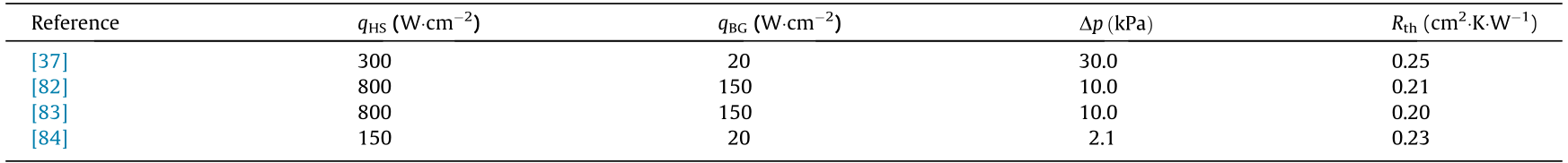
qHS: hotspot heat flux; qBG: background heat flux; Rth: thermal resistance;  : pressure drop.
《4.3. Immersion cooling (pool boiling)》
4.3. Immersion cooling (pool boiling)
Immersion cooling (via pool boiling) has recently received attention due to its associated energy savings and extended heat transfer limits. The heat transfer limits (both critical heat flux and boiling heat transfer coefficient) of pool boiling can be significantly enhanced by implementing boiling enhancement coatings (BECs) on top of the heated surface. As evident from Section 4 on fluid selection, water has been shown to be superior in terms of thermal performance (FOM).
Recent research efforts on immersion cooling via pool boiling aim to simultaneously maximize the boiling heat transfer coefficient (hb) and the critical heat flux (CHF). Patil and Kandlikar [85] demonstrated pool boiling enhancement using liquid water by selectively depositing a microporous coating on the fin tops of microchannels, resulting in a hybrid enhancement.
Since liquid water cannot directly come into contact with active devices, Birbarah et al. [9] employed an insulating dielectric layer over the active devices and employed water as the coolant. They reported an increased CHF with a moderate hb.
Xu and Zhao [86] demonstrated boiling enhancement by incorporating gradient metal foams employing the dielectric PF-5060. A detailed review of the pool boiling limits with BECs on the macroscale, microscale, and nanoscale can be found in Ref. [87]. Additively manufactured BECs are gaining interest due to their reduced contact resistance, which lead to much higher heat transfer limits (both CHF and hb). Many researchers have demonstrated that the use of 3D-printed BECs in the form of micro pin fins and mesh can simultaneously augment the CHF and hb. Wong and Leong [88] demonstrated that the 3D printing of BECs directly onto the heat surface can result in a CHF of 107 W·cm–2 , corresponding to a boiling heat transfer coefficient of 1.5 W·cm–2 ·K. MacNamara et al. [89] employed a solid-state additive manufacturing technology for BECs and demonstrated up to a 300% increase in CHF; they highlighted capillary wicking as an essential mechanism for enhanced boiling. Gess et al. [90] performed a system-level immersion cooling study using FC-72. Their immersion cooling tank design was versatile enough to serve in both flow and pool boiling experiments. The researchers employed microporous and microfinned BECs and reported 70% enhancement in CHF. A detailed summary demonstrating the effect of different BECs with optimal design guidelines is shown in Table 4 [91–99].
《Table 4》
Table 4 Summary of performance enhancement of nucleate pool boiling for different boiling enhancement methods.

PPI: pores per inch.
To gain an understanding of practical applications and feasibility, interested readers can see the work of Haghshenas et al. [100]. In that study, the researchers concluded that the efficiency of immersion-cooled data centers could be higher than that of traditionally air-cooled data centers. However, the researchers noted that a change in infrastructure could result in high cost. Ramakrishnan et al. [101] experimentally investigated the performance of air-, liquid-, and immersion-cooled data centers. They concluded that two-phase immersion and a cold plate provided the least thermal resistance.
Despite the use of cooling technologies and metal structures to enhance heat transfer as discussed above, there are some key design considerations for embedded cooling technologies:
(1) Optimal placement of the inlet and outlet manifold to improve the thermal resistance of the cooling solutions;
(2) Optimization of the fin or porous structures specific to the fluids to attain maximum heat transfer potential;
(3) Material selection to maximize thermal transport to enable advanced cooling solutions.
In general, a detailed optimization of the cooling solution can provide guidelines for the better co-design of embedded cooling solutions.
《5. Conclusions》
5. Conclusions
This paper provides a comprehensive review of published articles addressing embedded cooling via single-phase and twophase convection. Techniques such as etching microchannels, 3D printing of fins, and pool boiling enhancement by means of surface modification techniques are discussed.
(1) Embedded microchannels within a silicon chip using the dielectric coolant HFE-7100 can extend the heat dissipation capacity by up to 1020 W·cm–2 during uniform heating (thermal resistance: 0.07 cm2 ·K·W–1 ). Under simultaneous background and hotspot heating conditions, background heat fluxes of up to 900 W·cm–2 and hotspot fluxes of up to 2700 W·cm–2 can be dissipated.
(2) Printing fins on a chip can mitigate chip hotspots with a thermal resistance of 0.2 cm2 ·K·W–1 by employing single-phase liquid water at a pressure drop of 5 kPa.
(3) Two-phase immersion cooling via pool boiling with water and hybrid BECs can extend the CHF beyond 300 W·cm–2 (0.01 cm2 ·K·W–1 ). However, with dielectric fluid and gradient BECs, a critical heat flux of around 150 W·cm–2 (0.03 cm2 ·K·W–1 ) is achieved.
(4) Fluid selection is crucial in extending the heat transfer limits using embedded cooling. The conflict between lower GWP and superior thermal properties must be carefully resolved.
(5) This literature review also summarizes various boiling enhancement methods for immersion cooling via pool boiling. Each of the BECs have a significant impact on improving the thermal performance. BEC fabrication via additive manufacturing is an emerging technology.
Embedded cooling, as defined here, would eliminate several sources of thermal resistances. Still, incorporating embedded cooling often simultaneously requires the introduction of new and rarely practiced approaches such as exposing the devices to direct contact with liquids or two-phase systems. Another primary consideration is that embedded solutions usually require changes to be made to the device-manufacturing infrastructure, which is prohibitively expensive. These reasons explain why the disclosed and patented solutions in this field are rarely practiced in mainstream manufacturing. Which embedded cooling strategies are adopted and when this will occur depend on industry requirements (e.g., a need for higher heat fluxes to meet performance targets, requirements for compact package sizes, and/or closer integration of components) and on which technologies meet these requirements with the least perceived disruption, risk, and expense. Some combination of passive and active cooling solutions is likely, given current electronic and packaging trends.
《6. Future work》
6. Future work
In terms of thermal management by means of embedded cooling, two-phase dielectric coolants are considered to provide the maximum heat flux dissipation with the minimum wall super heat. Future efforts could focus on developing simpler computational models to predict flow boiling characteristics and instabilities in order to help better design two-phase boiling-based embedded cooling designs. Improved modeling capabilities will also help aid co-design. The use of localized jet impingement cooling to remove high heat fluxes is gaining traction. Detailed AI-driven optimization to route the flow efficiently in order to impinge on the hotspots will be of interest in future. Furthermore, serious life-cycle assessments of such embedded cooling technologies are necessary in order to better understand the opportunities and challenges associated with their future implementation. There is also a need to develop FOMs to evaluate the risk associated with embedding cooling solutions onto the device.
《Acknowledgments》
Acknowledgments
This work was supported by National Science Foundation (1941181), National Science Foundation (1846157), Semiconductor Research Corporation CHIRP (Task 2878.006), and Department of Defense (13000844-021).
《Compliance with ethics guidelines》
Compliance with ethics guidelines
Srikanth Rangarajan, Scott N. Schiffres, and Bahgat Sammakia declare that they have no conflict of interest or financial conflicts to disclose.


 京公网安备 11010502051620号


