
2013, Volume 15, Issue 1
Strategic Study of CAE >> 2013, Volume 15, Issue 1
Fabrication and characterization of typical nano-scale structures
1. School of Mechanical Engineening, Xi'an Jiaotong University, Xi'an 710049, China;
2. State Key Laboratory for Manufacturing Systems Engineering, Xi'an Jiaotong University, Xi'an 710049, China
Next Previous
Abstract
Three types of nano-scale structure have been fabricated and characterized using SEM, AFM, etc. In this paper, multilayer thin film deposition technique has been used to fabricate nano-scale structure with 20nm, 25 nm and 35 nm line-width. LER and LWR of nanoline are evaluated with an offline image analysis algorithm. The experimental results indicate that the LER/LWR of the lines is low and the uniform of the lines is high. EBL and ICP technique are employed to fabricate grating patterns with nominal height 220 nm. The result shows that the high frequency fluctuations of line edges after etching decrease, the correlation length increases and values of root mean square deviation (σ) increase. Single and multiple nano steps have been fabricated using FIB technique, and the relationship between the size of the Z-axis and energy of process are analyzed.
Figures
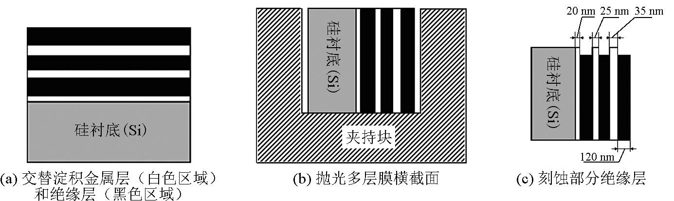
图1
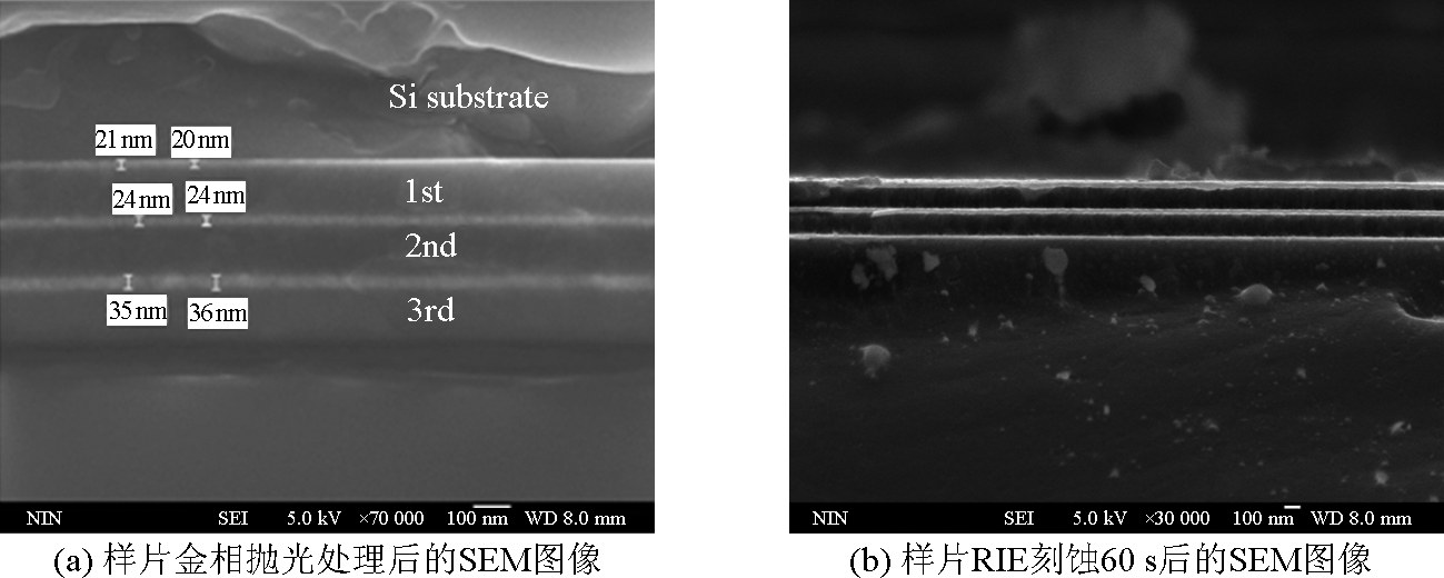
图2
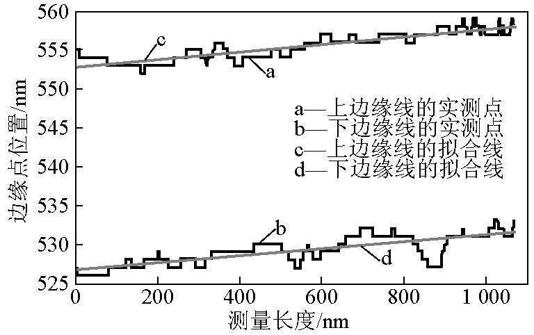
图3

图4
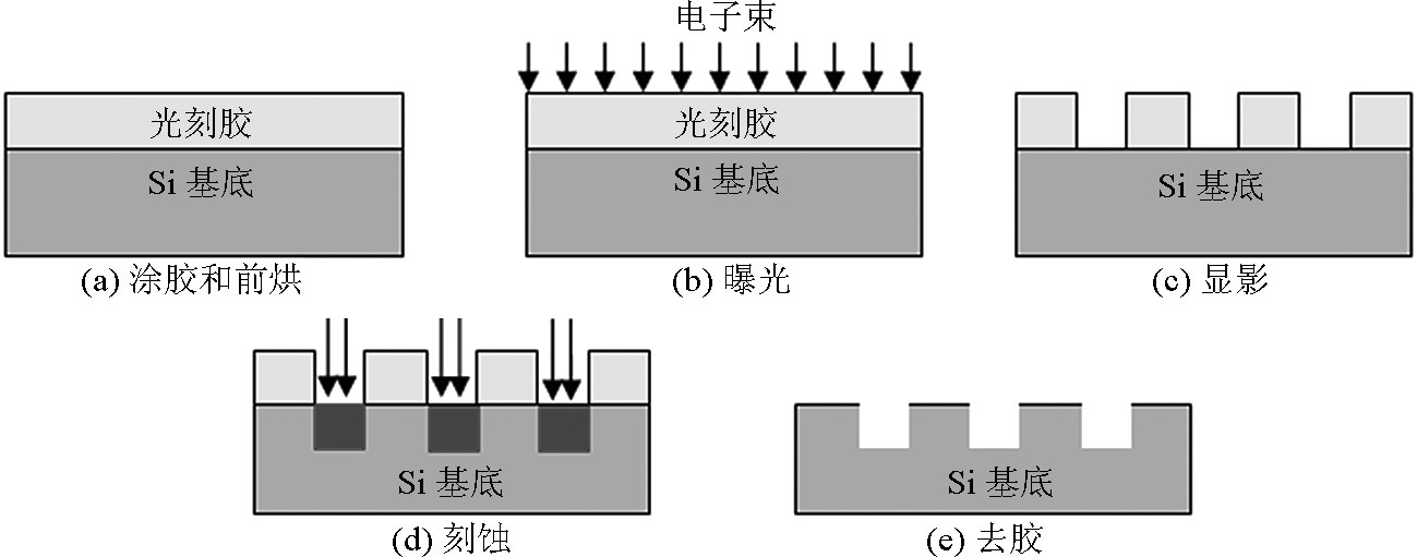
图5

图6
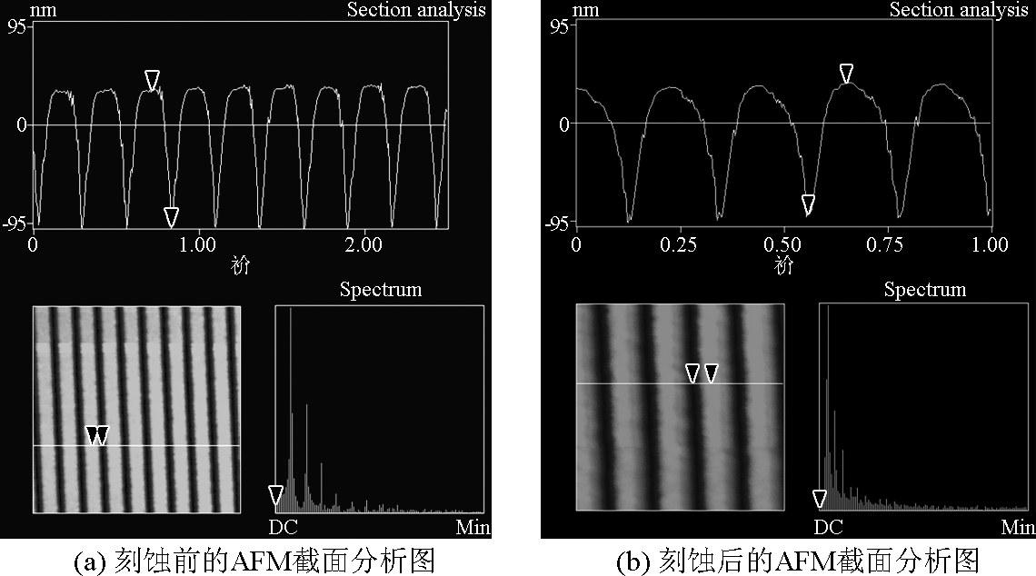
图7

图8
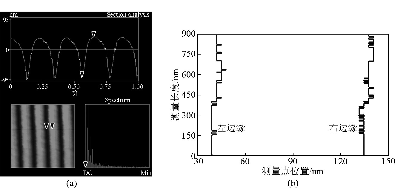
图9
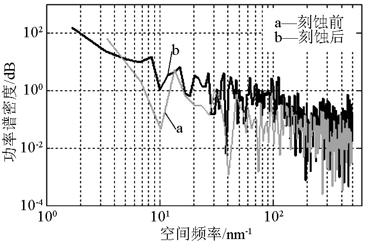
图10

图11

图12
References
[ 1 ] Dixon R G,Koening R G,Fu J,et al. Accurate dimensional metrology with atomic force microscopy[J]. Proc. of SPIE,2000, 3998:362-368. link1
[ 2 ] Zhao F,Jiang Z,Jing W,et al. Fabrication and characterization of sub-45 nm multiple linewidth samples[J]. Meas. Sci. Technol., 2007,18:1689-1693. link1
[ 3 ] Tortonese M,Prochazka J,Konicek P,et al. 100 nm pitch standard characterization for metrology applications [C]. Proc. of SPIE,2002,4689:558-564. link1
[ 4 ] Frase C G,Buhr E,Dirscherl K. CD characterization of nanostructures in SEM metrology [J]. Meas. Sci. Techno.,2007,18: 510-519. link1
[ 5 ] Gogolides E,Constantoudis V,Patsis G P,et al. A review of line edge roughness and surface nanotexture resulting from patterning processes [J]. Microelectron. Eng.,2006,83:1067-1077. link1
[ 6 ] Tortonese M,Guan Y,Prochazka J. NIST- traceable calibration of CD-SEM magnification using a 100 nm pitch standard [C]. Proc. of SPIE,2003,5038:711-718. link1
[ 7 ] Chen Z,Gao S,Lu M,et al. Step height measurement by the metrological atomic force microscope [J]. Chinese Journal of Nanotechnology and Precision Engineering ,2008,6(7):288-292.
[ 8 ] Huang X,Han L,Gu W. Research of figures with high aspect ratio made by electron beam lithography system [J].Chinese Journal of Transducer Technology,2004,23(11):30-31.
[ 9 ] Guo T,Hu C,Chen J,et al . Five-frame phase-shifting algorithm for nanoscale step characterization [J].Chinese Journal of ACTA Metrological Sinica,2007,28(4):302-305. link1
[10] Xu Z,Fang F,Zhang S,et al. Fabrication of complicated micronano structures using focused ion beam milling method[J]. Journal of Tianjin University,2009,42(1):91-94. link1
[11] Yariv D,Yuval G,Amir R. Strategy for focused ion beam compound material removal for circuit editing[J]. American Vacuum Society,2012,011207:1-9. link1
[12] Walke J F R,Moore D F,Whitney J T. Focused ion beam processing for microscale fabrication[J]. Microelectronic Engineering,1996,30:517-522. link1


 京公网安备 11010502051620号


